
I’ve been meaning to learn the Android development environment but was not excited about leaving my beloved NetBeans IDE. Fortunately, there is the NBAndroid plugin that, together with the Android SDK, allows you to easily develop and test Android apps using NetBeans. Next up, go through (and report on) some Android tutorials.
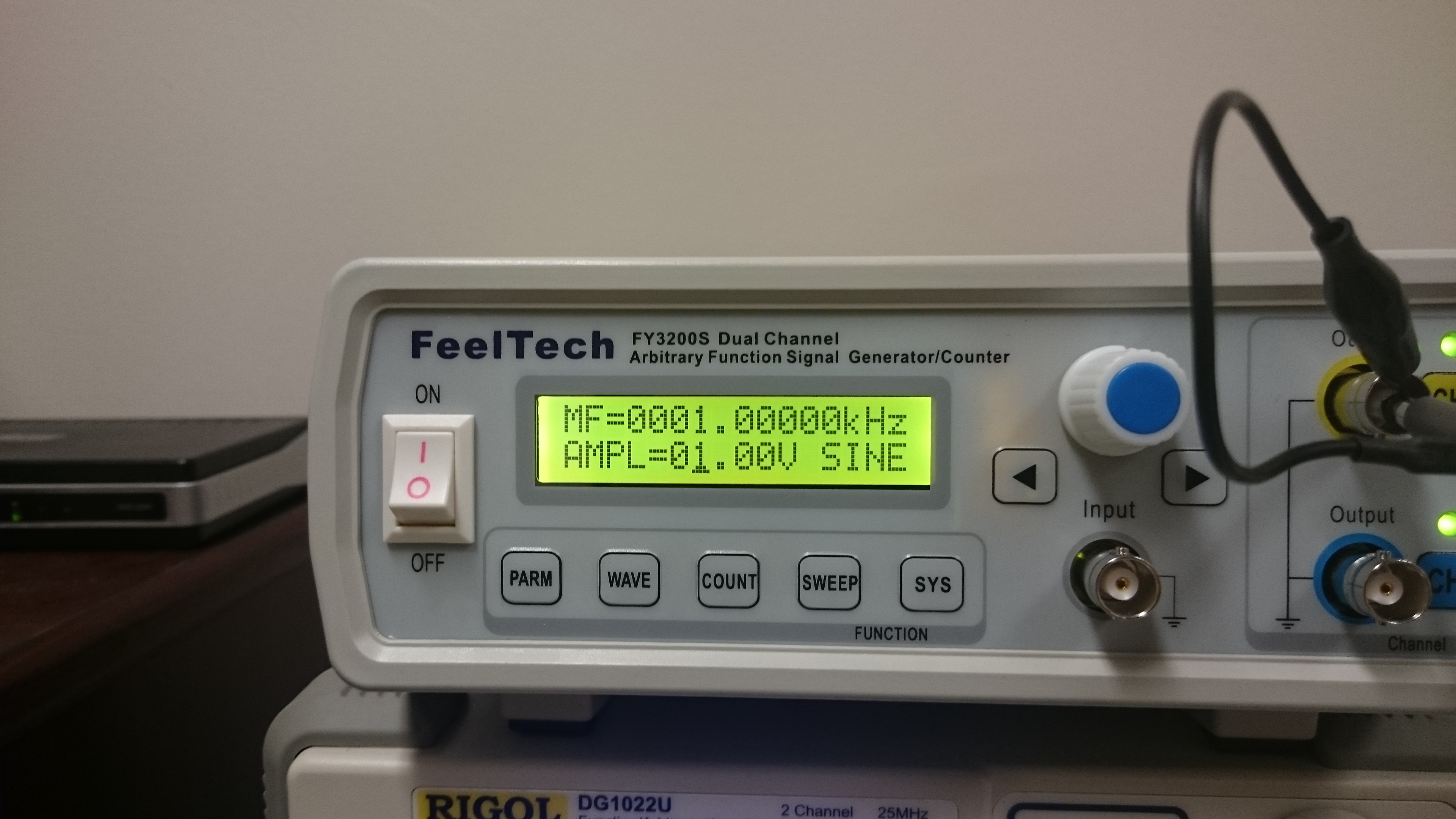
Feeltech FY3200S Signal Generator
Update 8/3/2017:
It looks like there’s a new low-cost signal generator option that appears significantly better than the Feeltech. The Ruideng JDS6600 comes in version from 15MHz ($78) – 60MHz ($122) and has a control panel that is much nicer; more like the Rigol and Siglent low-end signal generators but at a significantly lower price point. I haven’t tried these yet, but next time I’m buying an inexpensive signal generator, that will be the one.
Update 5/4/2016:
I replaced the AC power jack with a 3-prong jack and connected the earth/safety ground to the DC ground and now the DC ground is (of course), at earth/safety ground potential and there is no unwanted/unexpected AC voltage on the outputs so I am once again pleased with this signal generator/frequency counter. The cost of the replacement jack is low
Update 4/23/2016:
I’ve ordered a 3-conductor AC socket that was suggested as an easy-to-fit replacement for the 2-condoctor socket on the FY3224S; the socket is available from amazon and ebay (note: both are very slow shipping). When it arrives, I’ll replace the existing AC socket and connect the DC ground to AC safety/earth ground. I’d rather have the output truly float, but I think this is an acceptable solution.
Update 3/10/2016:
I got a mild shock from my FY3224S today; the problem appears to be with the mains filter implementation. Measuring between the BNC connectors (DC ground) and the AC earth ground I see an 82v peak-to-peak signal. For more information see eevblog here. The signal is low current when the unit is on (around 32uA) which is well below the 250uA limit for such gear. There’s 110vac at around 50uA on the DC ground (the exposed metal connectors) when the unit is off. I think this is not dangerous, but it’s nothing I’d want to connect to the sensitive circuits I’d use a signal generator to feed. The issue is that the power supply is Class II (no earth ground) and there’s an EMC reduction capacitor that bridges the HV and SELV sides of the transformer. AC current leaks through this capacitor to the DC output connectors. From my perspective this is unacceptable for electronic test equipment as it could easily damage whatever it is connected to if that equipment is earth referenced. Until this is resolved, I can’t use or recommend this signal generator to anyone.
——————————————————
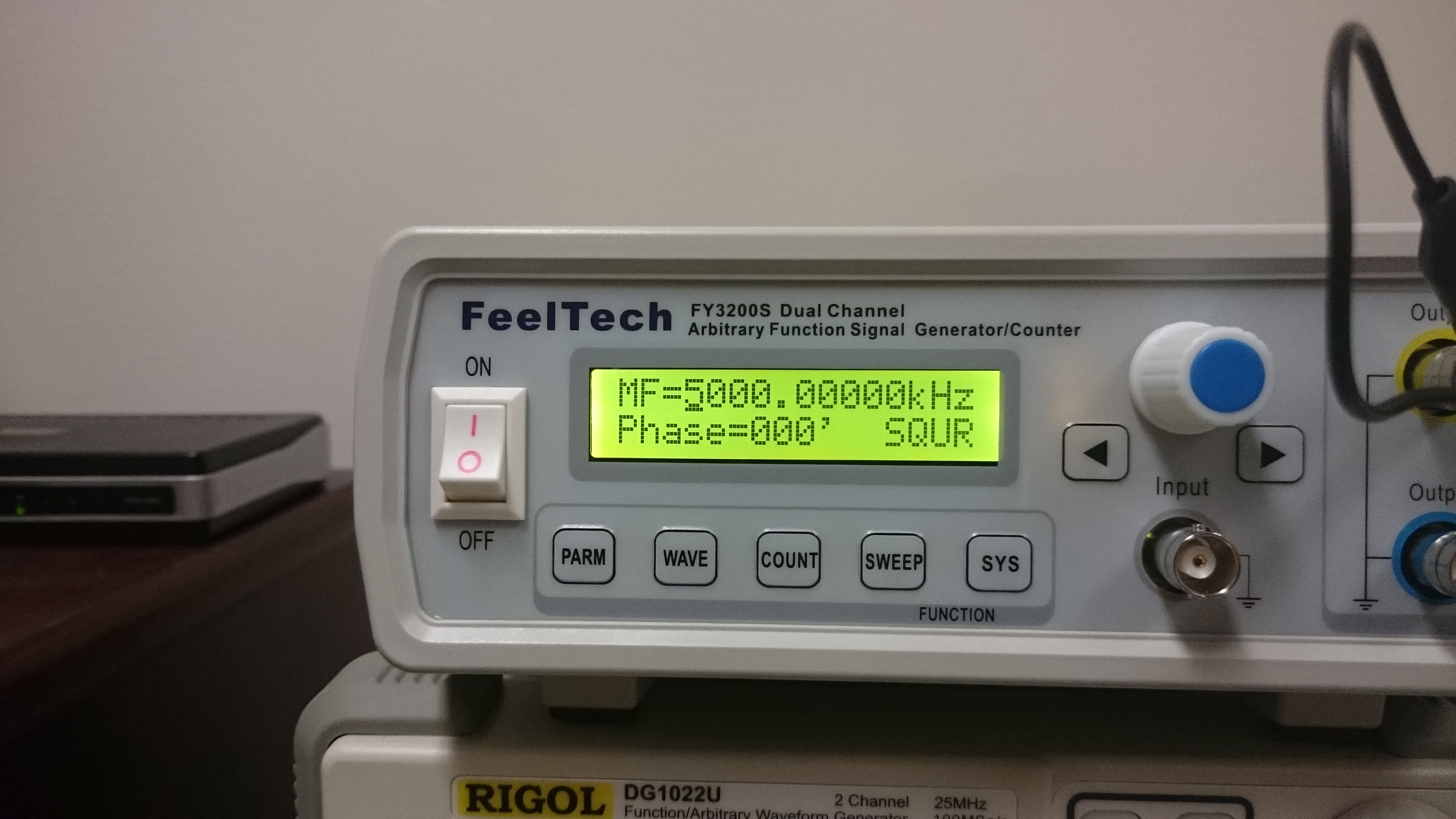
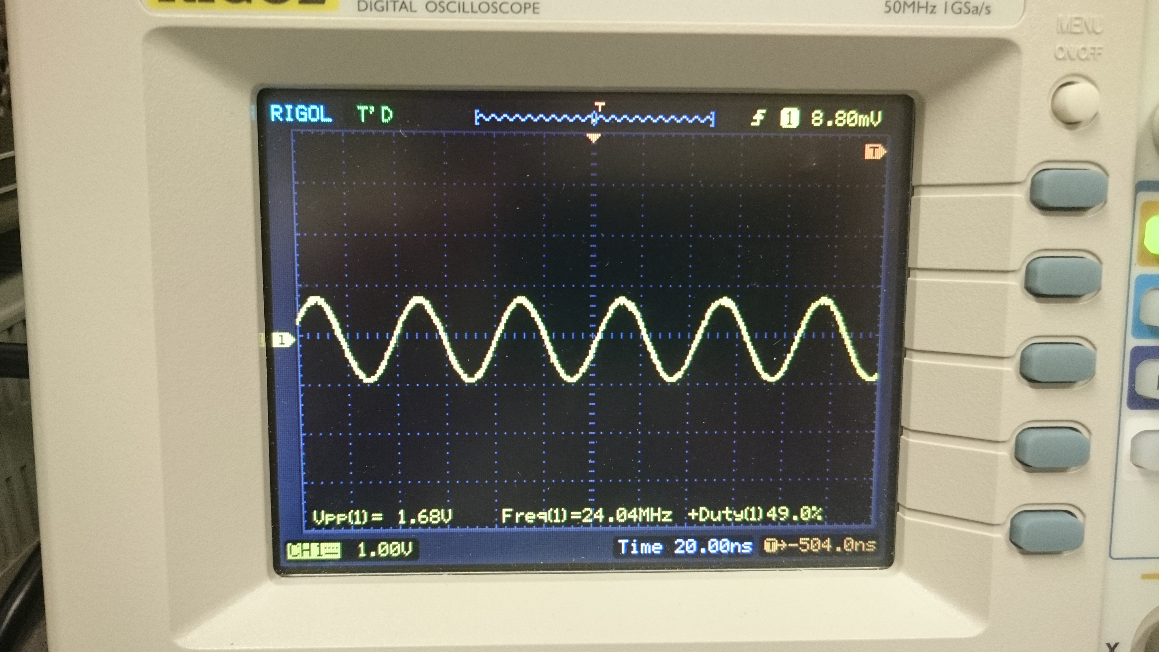
I wanted a second signal/function generator to use at home and couldn’t resist buying a Feeltech FY3200S. They are commonly available for under $80 shipped on eBay and claim to generate waveforms at up to 24MHz. It arrived today and I did a quick head-to-head comparison between it and my Rigol DG1022 signal generator. The Rigol is a 25MHz generator and I’ll say up front that it is a joy to use and looks and feels like a real piece of lab equipment; however it also costs nearly 5x as much as the Feeltech.
The FY3200S is a DDS generator with a claimed 250MS/s rate so it
FY3200 Signal Generator
should do a serviceable job of generating sine waves at up to 24MHz (I consider 10 points per cycle the minimum). The FY3200S lets you control the waveform either from your computer using software and a standard USB A-B cable or via a front panel with 2-line LCD display, several membrane buttons and a rotary encoder (dial). Interaction is straightforward, but clunky compared to the Rigol. Unfortunately the USB cable does not power the generator. You must power the generator via its 2-conductor AC cable (universal 85v-260vac).
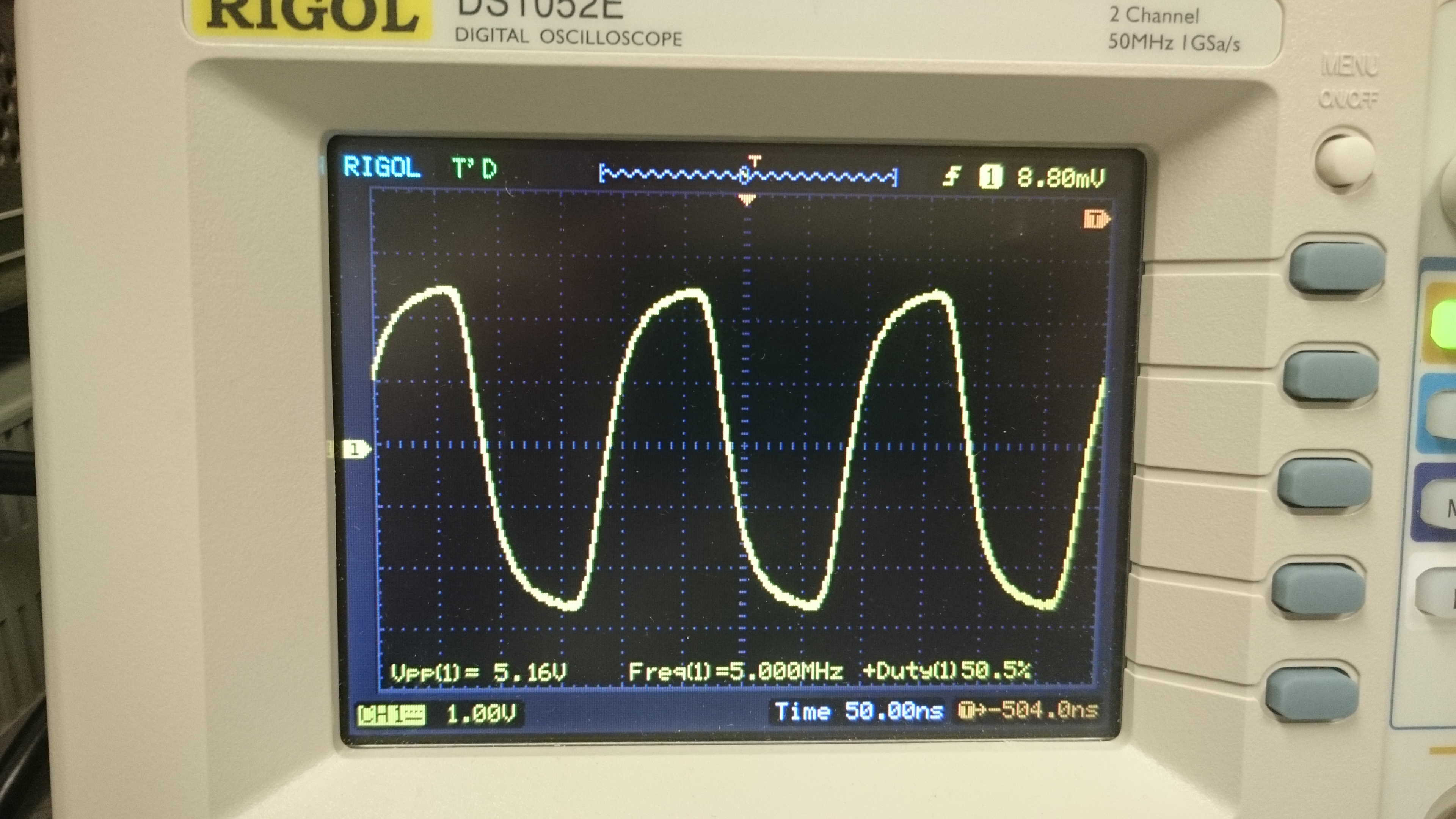
I have been disappointed by other low cost DDS generators, particularly at higher frequencies. Because it is DDS, I expect good frequency accuracy (which it has). The big questions in such a low cost device are waveform stability (jitter) and how the analog output stage performs at higher frequencies. So I ran a few tests to see when the analog output would fall apart. The output was connected to my Rigol DS1052 (50MHz hacked to 100MHz) oscilloscope so there was no load on the generator (I’ll test again with a 50-ohm load later).
I also tested the software that lets you control the generator via USB from your computer and it worked well.
The FY3224S includes a frequency counter rated for 100MHz. Depending on the signal level, mine was able to measure signals accurately up to 225MHz (at +13dBm) which was pretty impressive for a device this inexpensive.
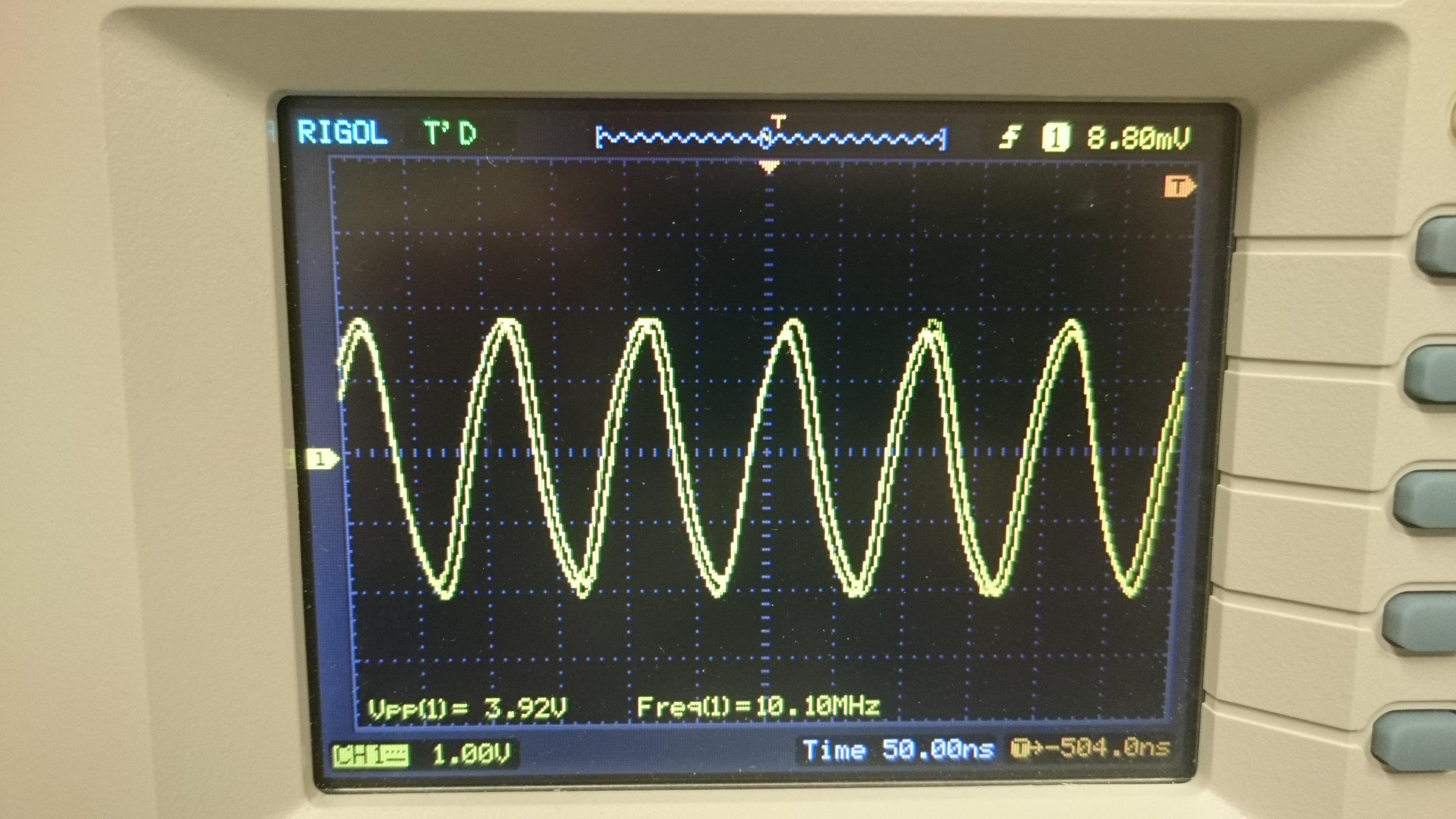
On to the tests: I configured the generator for a 1kHz 1v sine wave and gradually raised the frequency while observing the amplitude. As you can see, it held together nicely through about 3MHz and then started to drop. Clearly the GBW of the output buffer (likely a low cost op-amp) is not sufficient for the higher frequencies; I’ll probably open it up later to see if it can be replaced with a better op-amp. Looking only at frequencies above 1MHz:
1MHz = 1v03
2MHz = 1v01
3MHz = 0v98
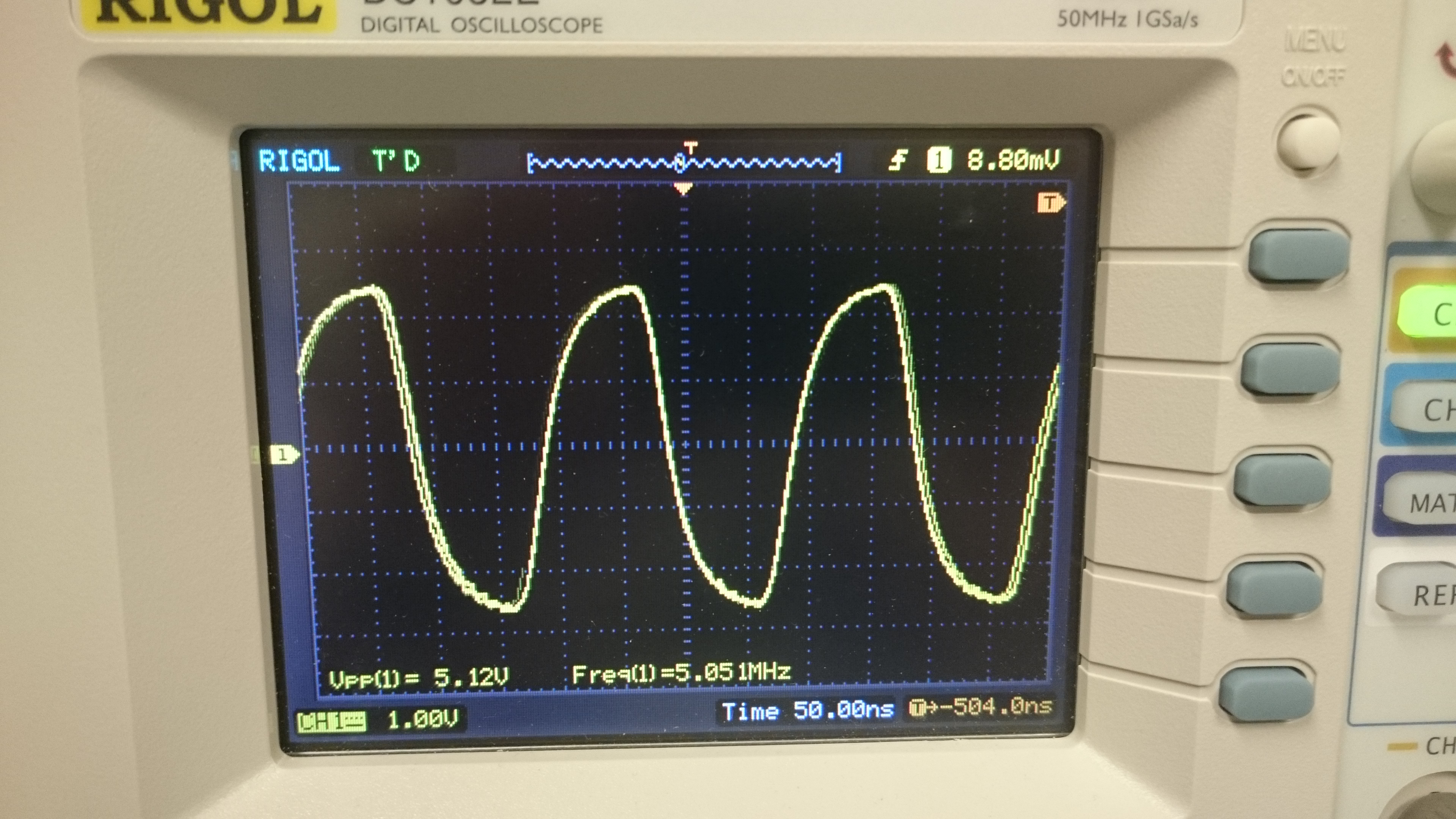
5MHz = 0v86
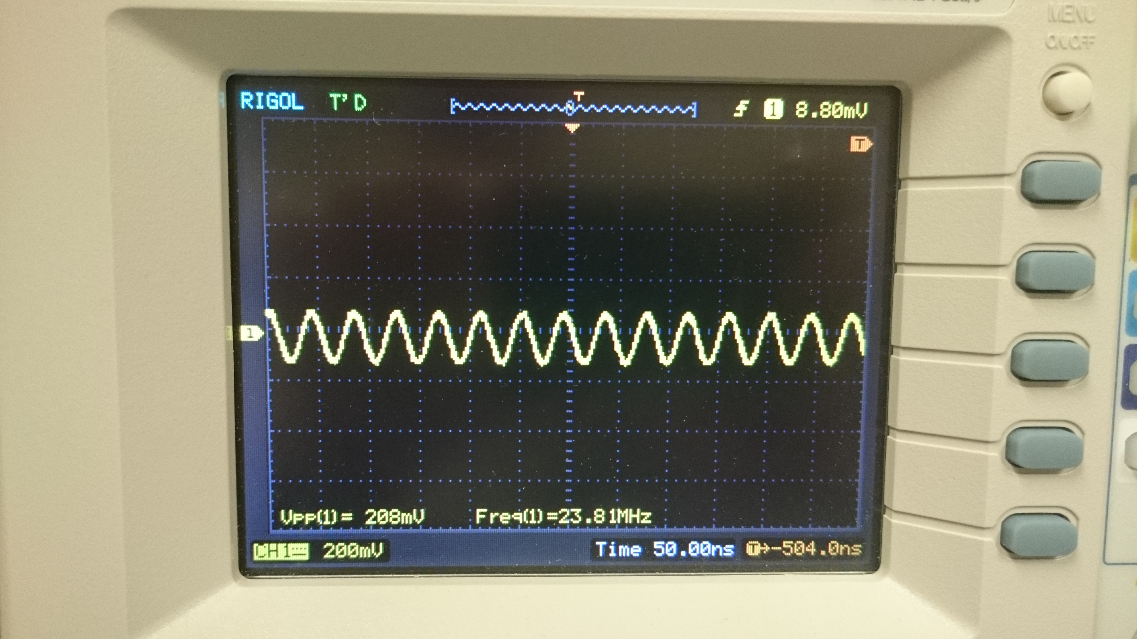
10MHz = 0v59
15MHz = 0v42
20MHz = 0v29
24MHz = 0v21
Stability and shape of the sine wave was good across the entire range of frequencies. At higher frequencies, the digital steps were clear as jaggies in the signal; the output filter could provide better smoothing, but overall it was pretty good…not as good as the Rigol, but still decent. I need to run some more tests with the output connected to a spectrum analyzer.
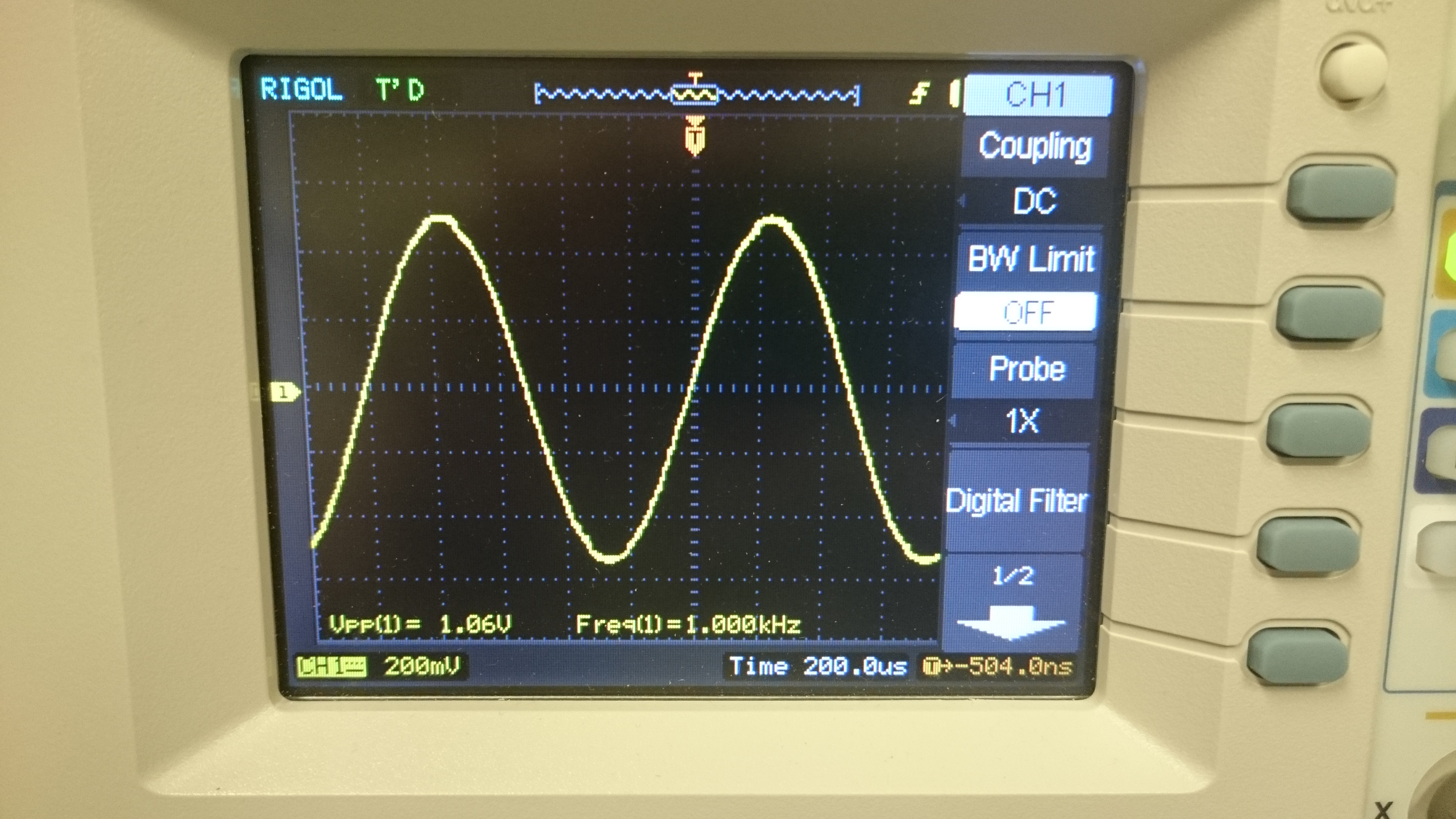
FY3200S 1KHz 1V Sine
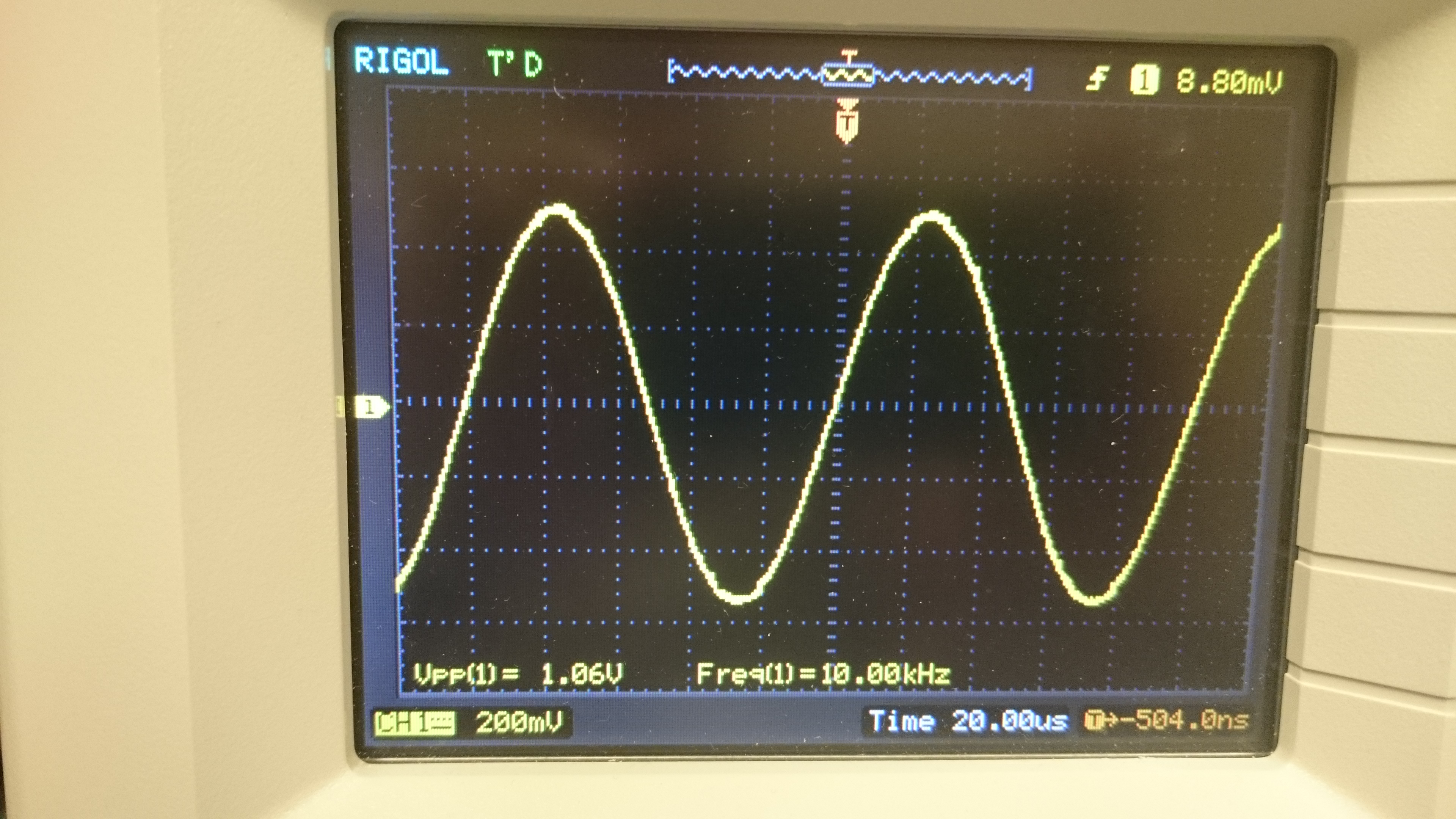
FY3200S 10KHz 1V Sine
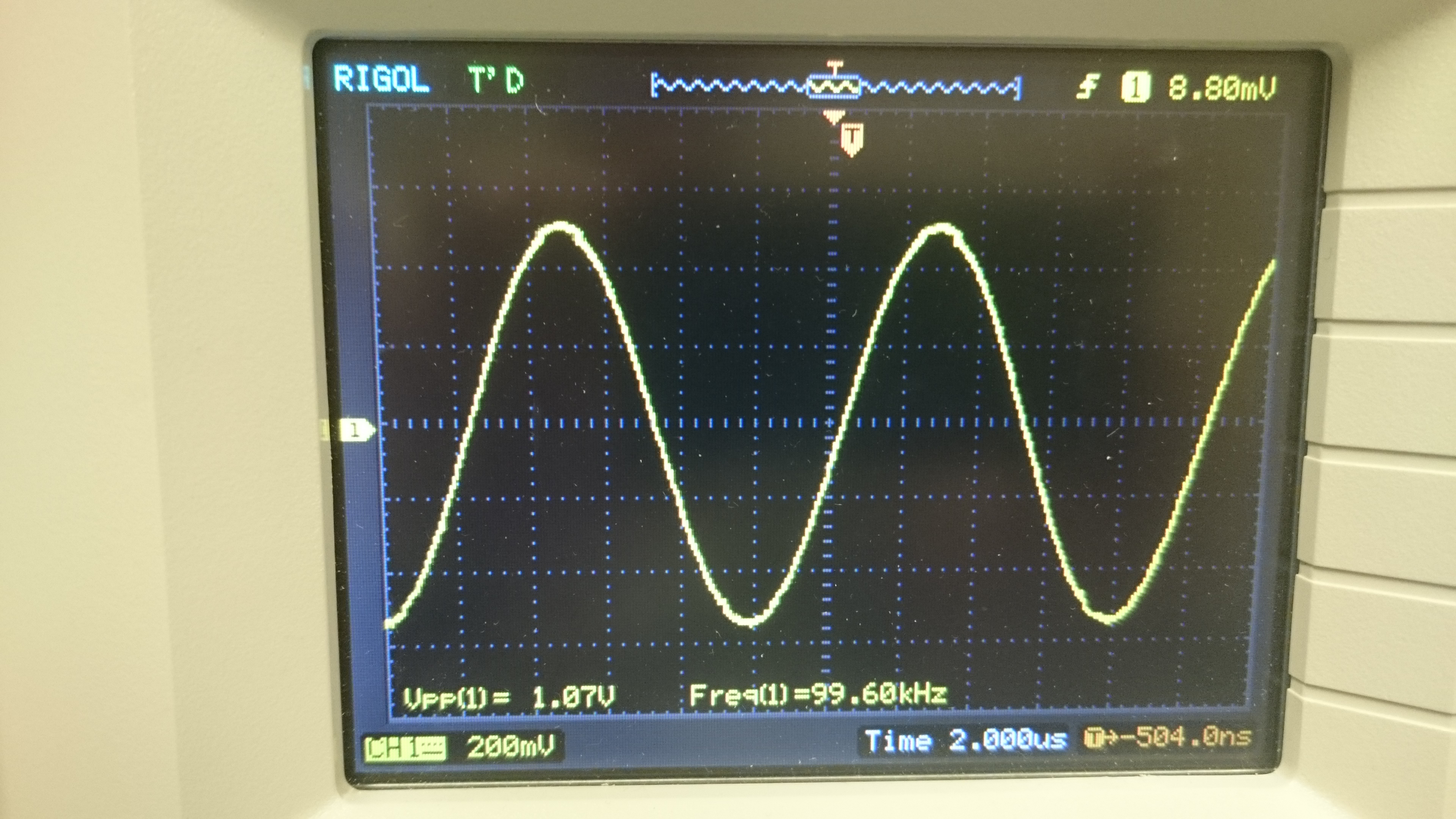
FY3200S 100KHz 1V Sine
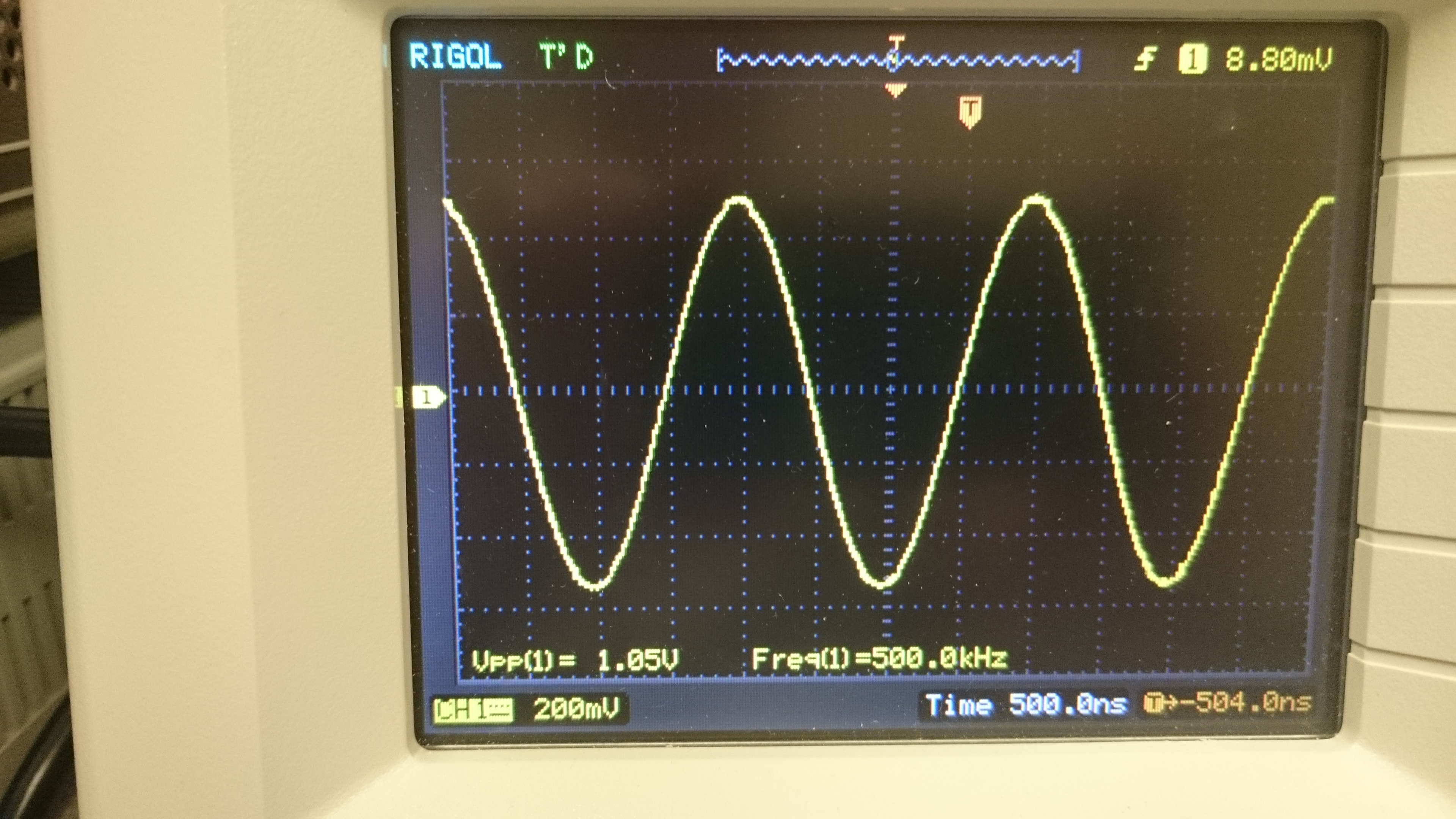
FY3200S 500KHz 1V Sine
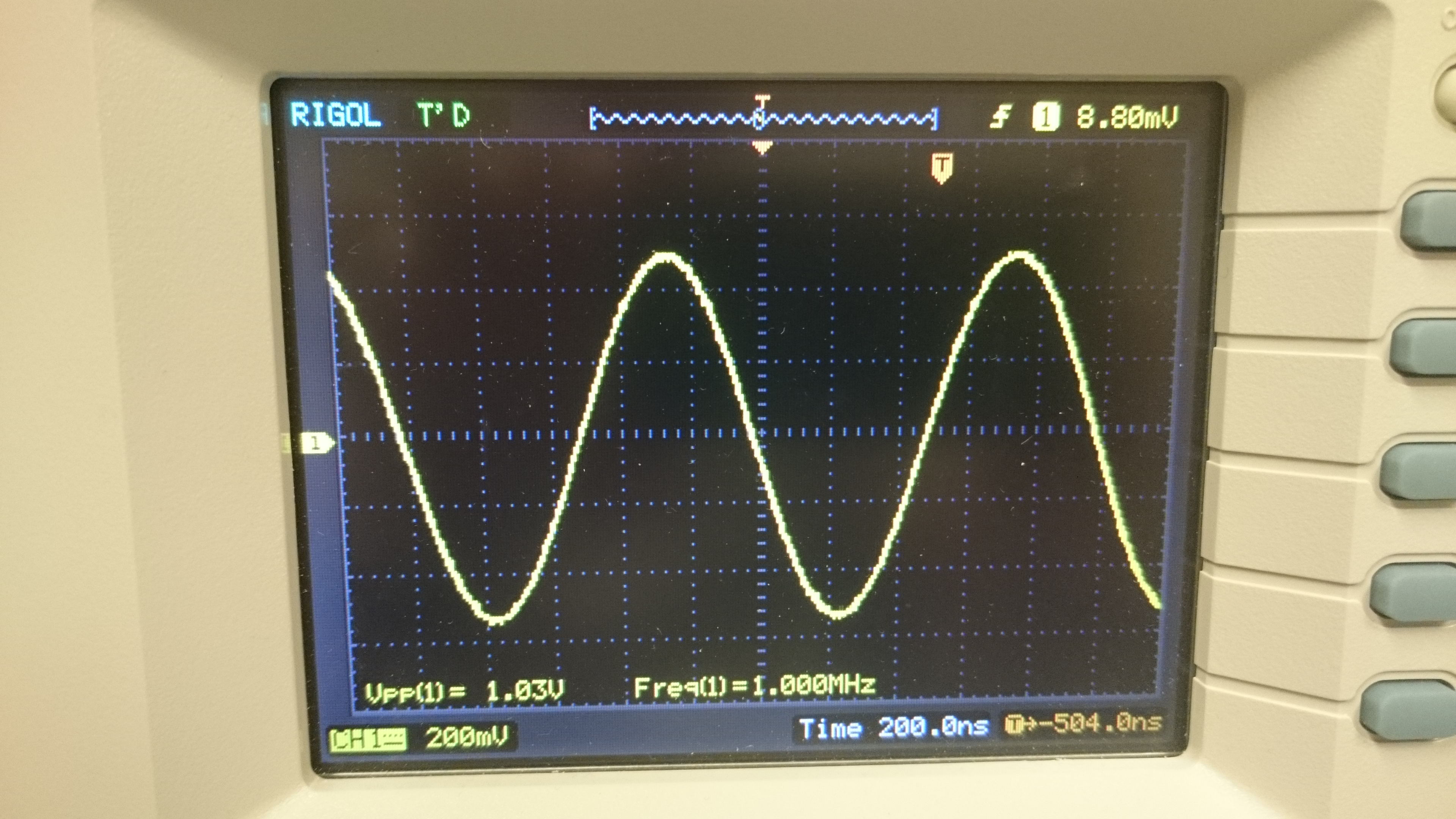
FY3200S 1MHz 1V Sine
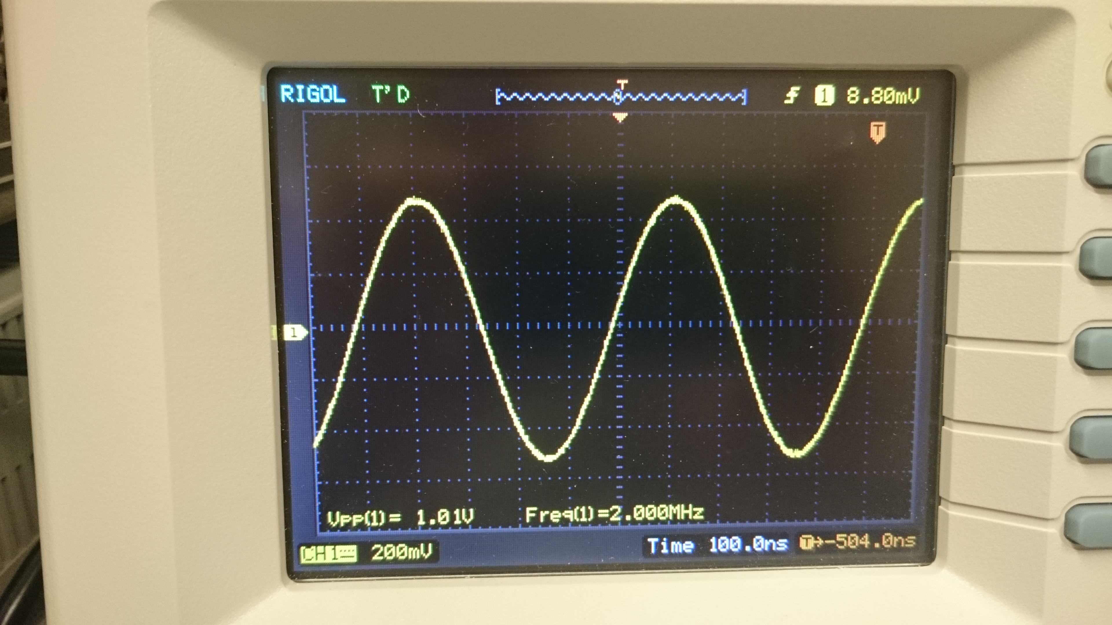
FY3200S 2MHz 1V Sine
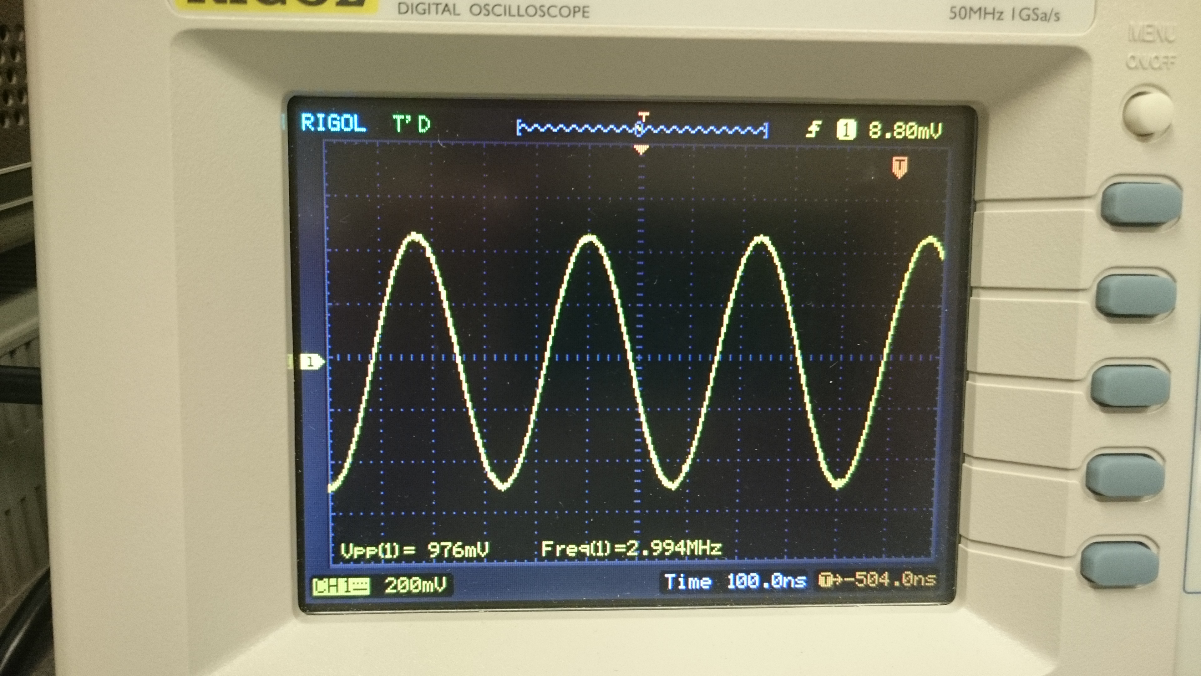
FY3200S 3MHz 1V Sine
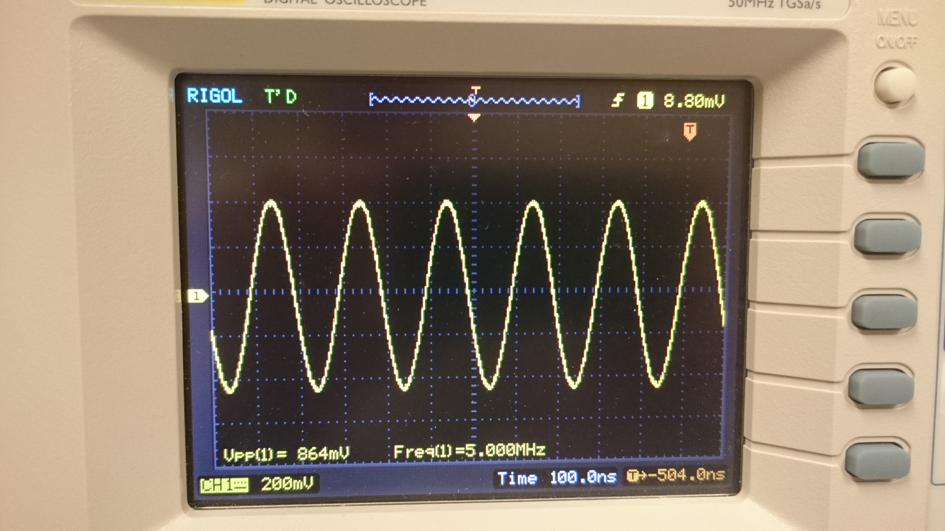
FY3200S 5MHz 1V Sine
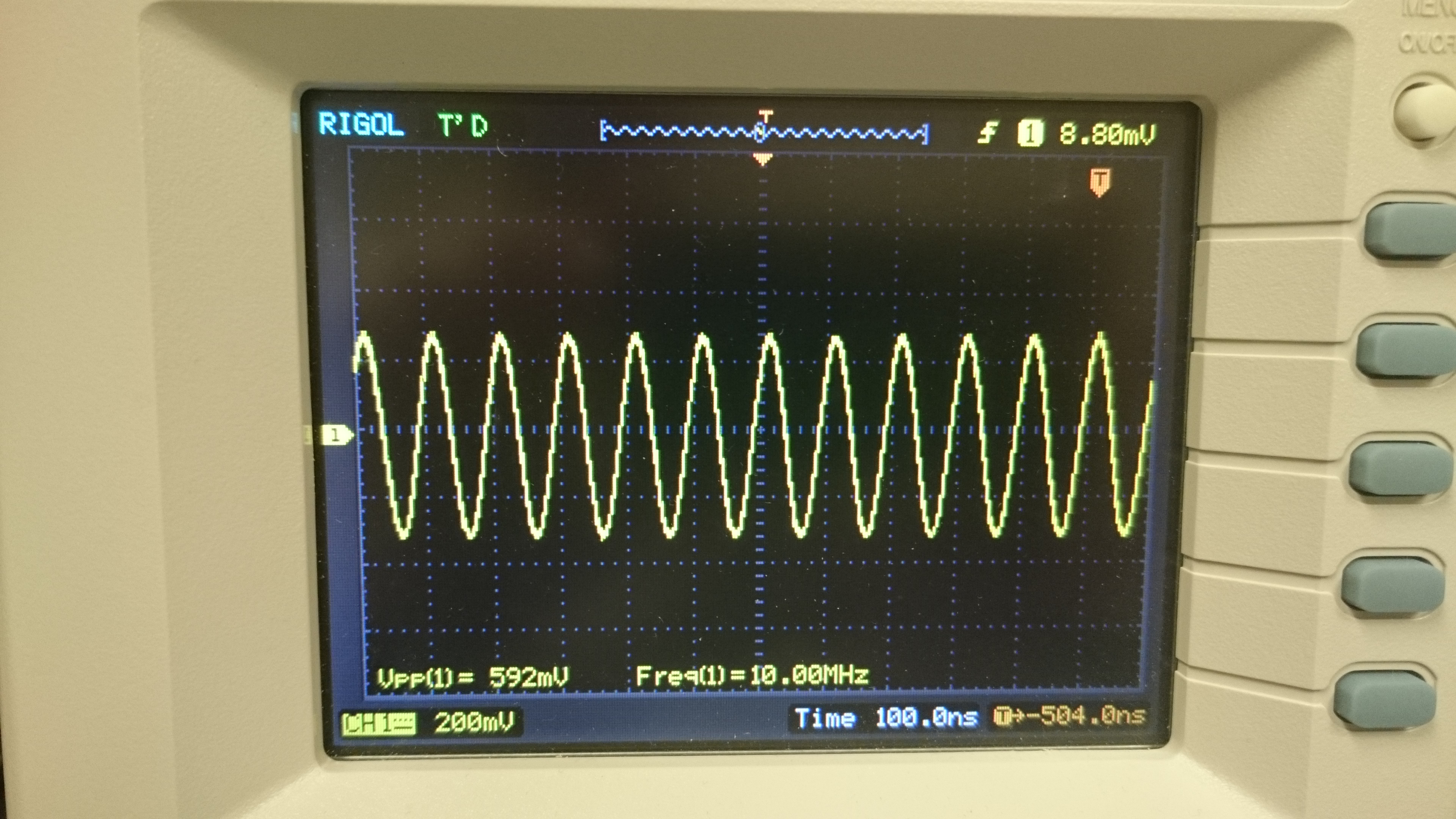
FY3200S 10MHz 1V Sine
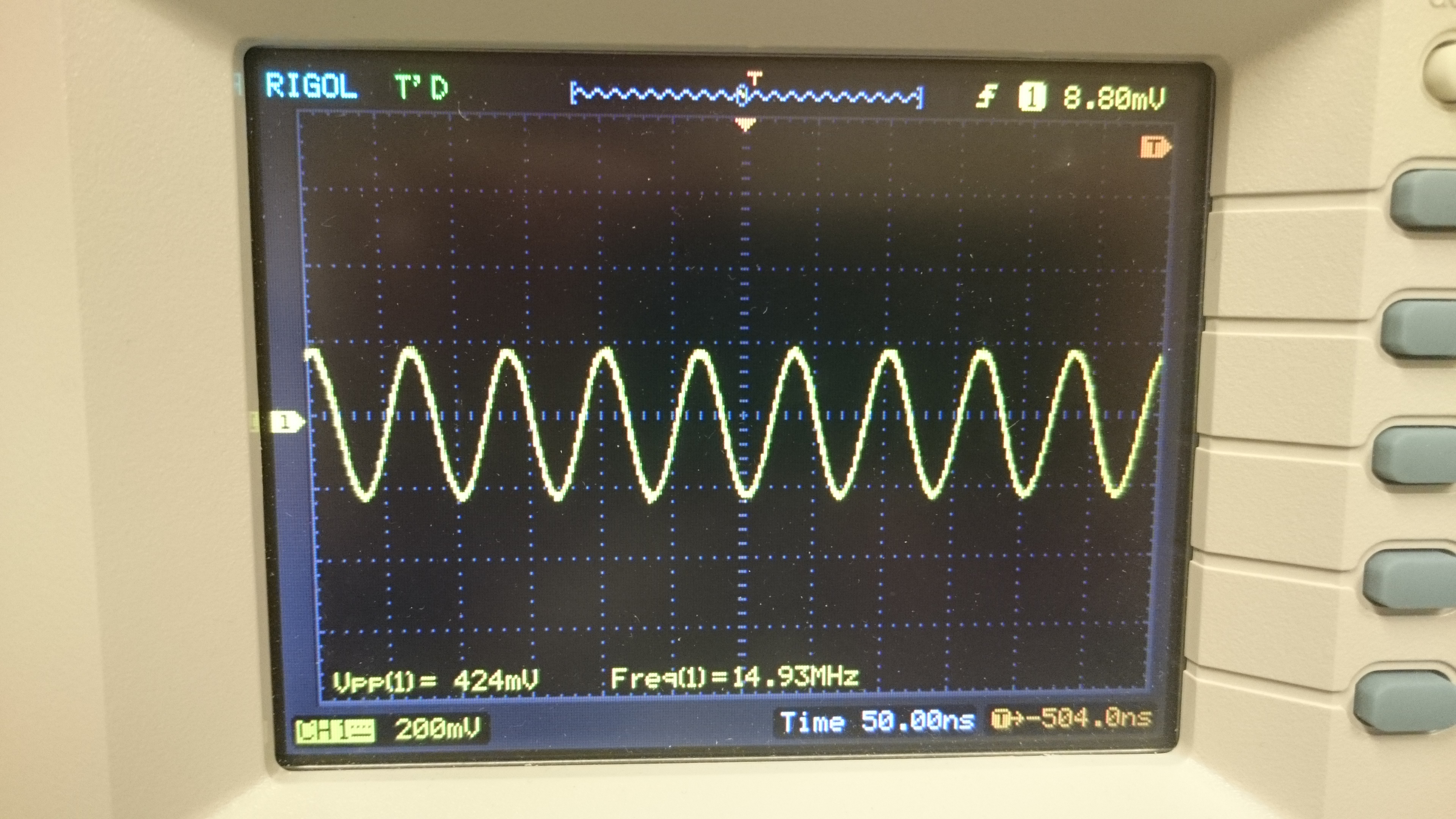
FY3200S 15MHz 1V Sine
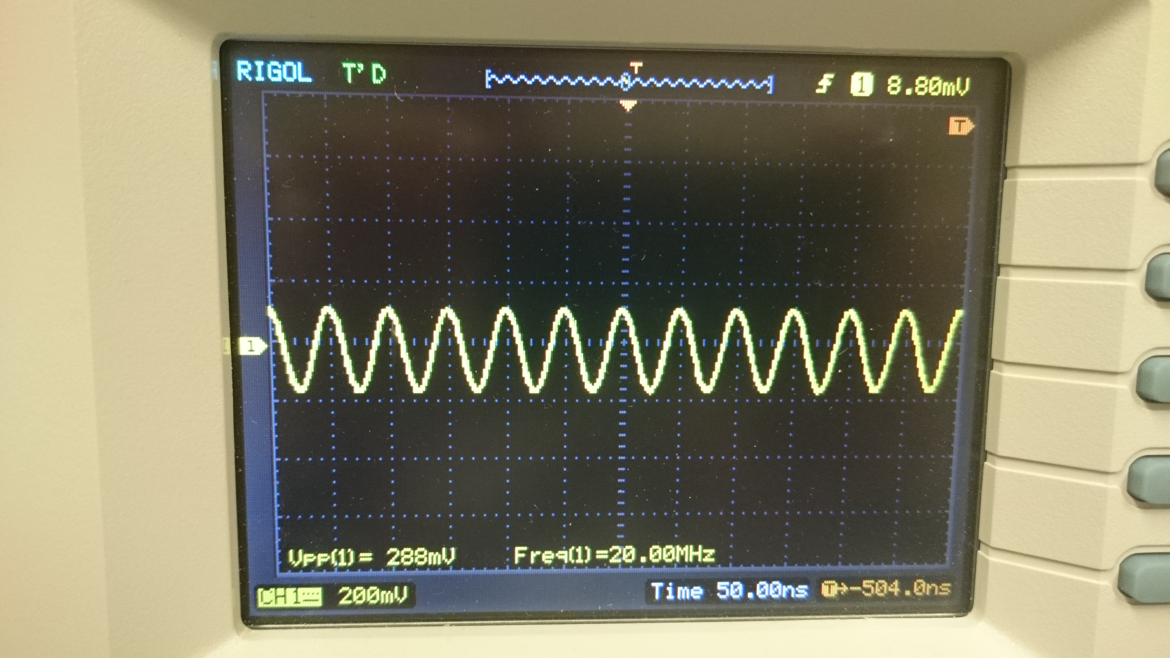
FY3200S 20MHz 1V Sine
FY3200S 24MHz 1V Sine
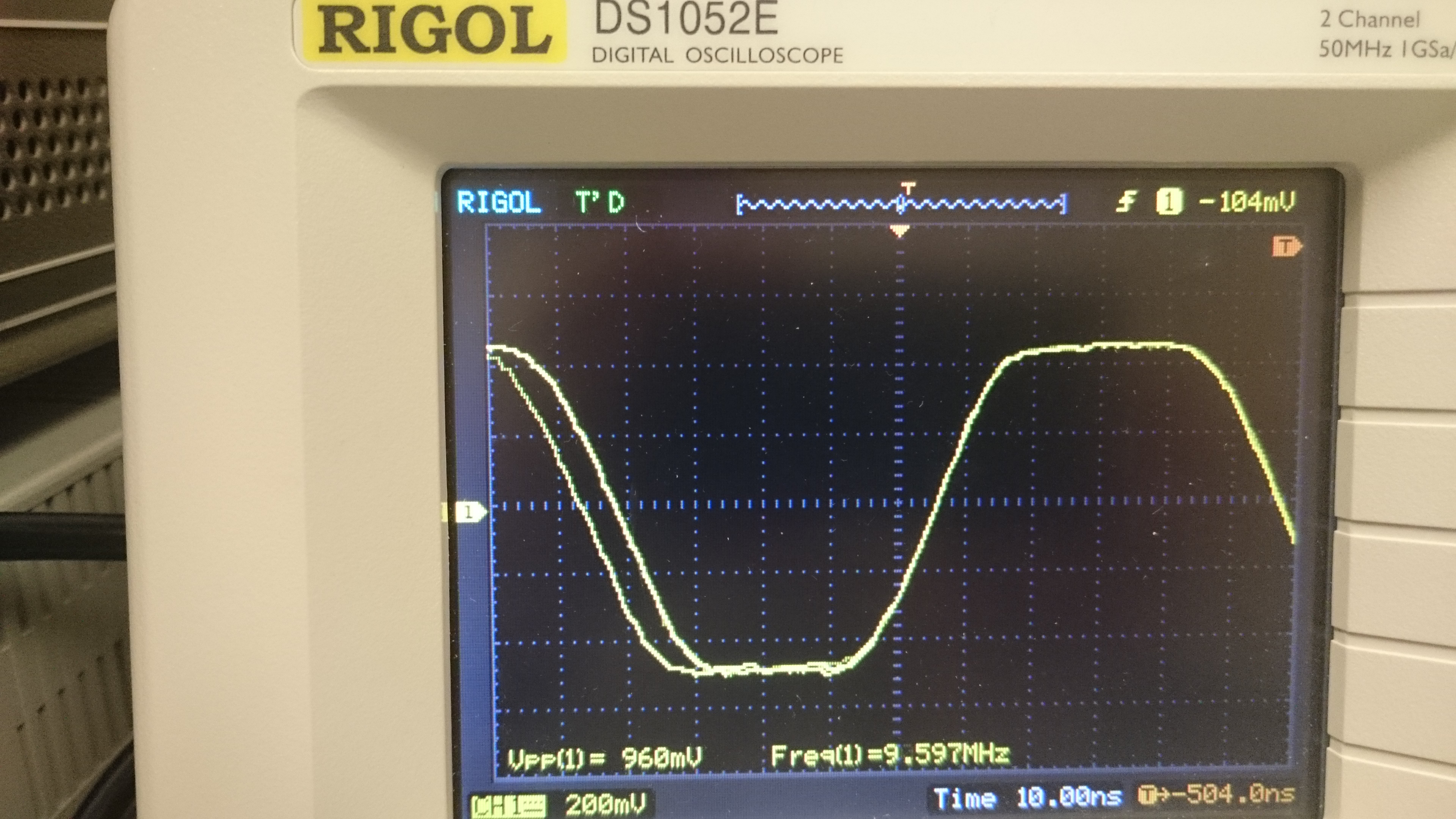
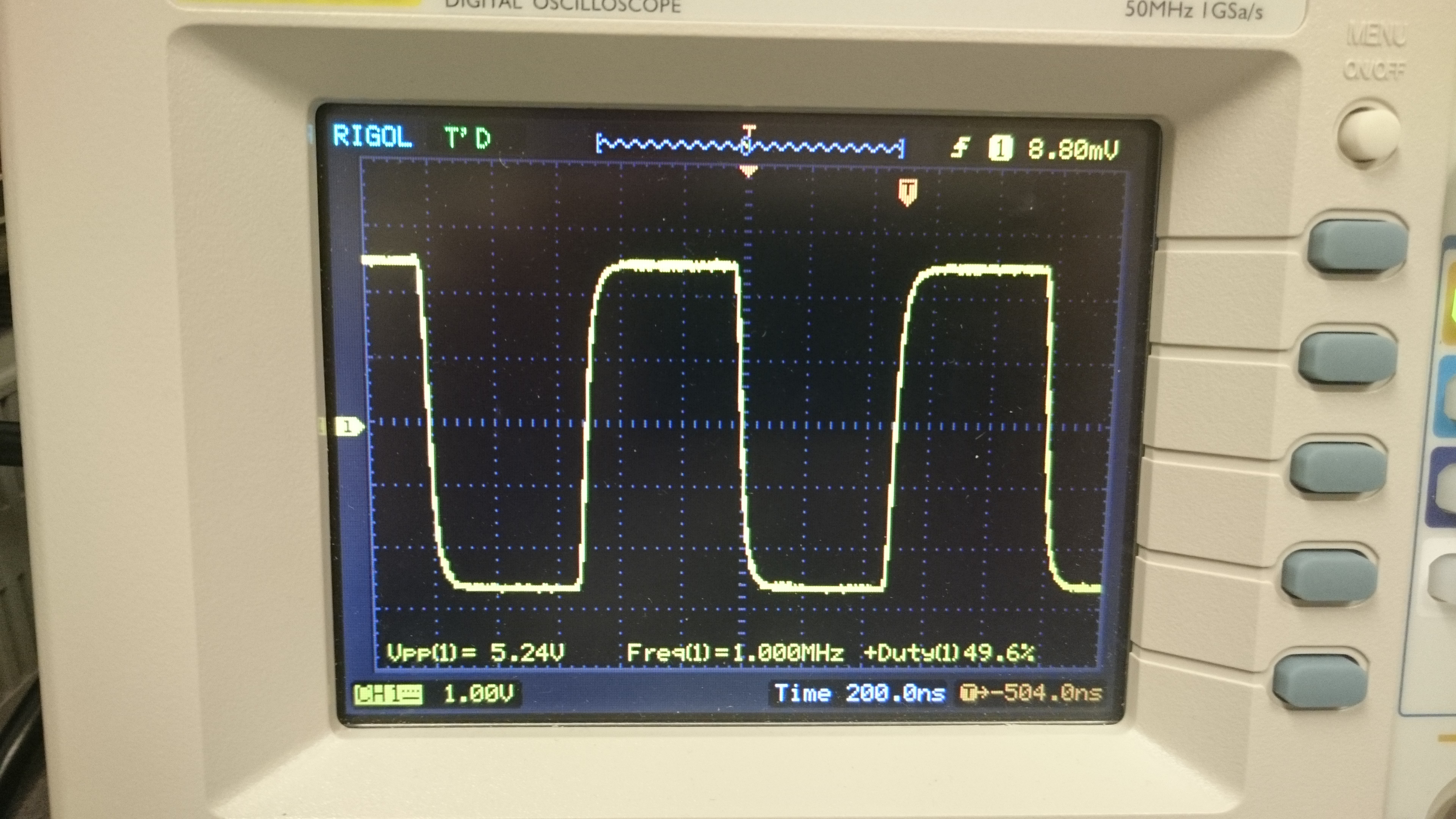
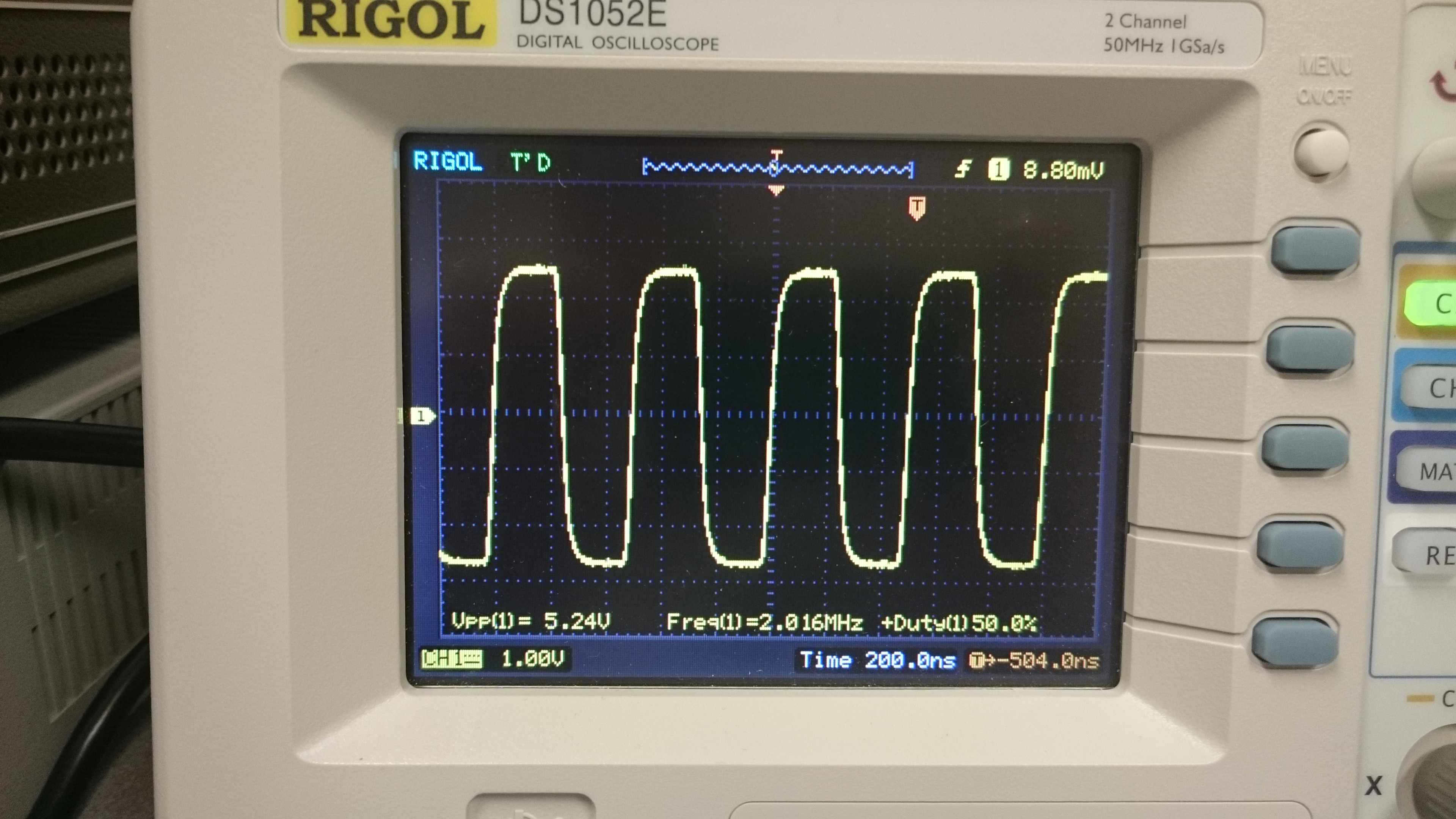
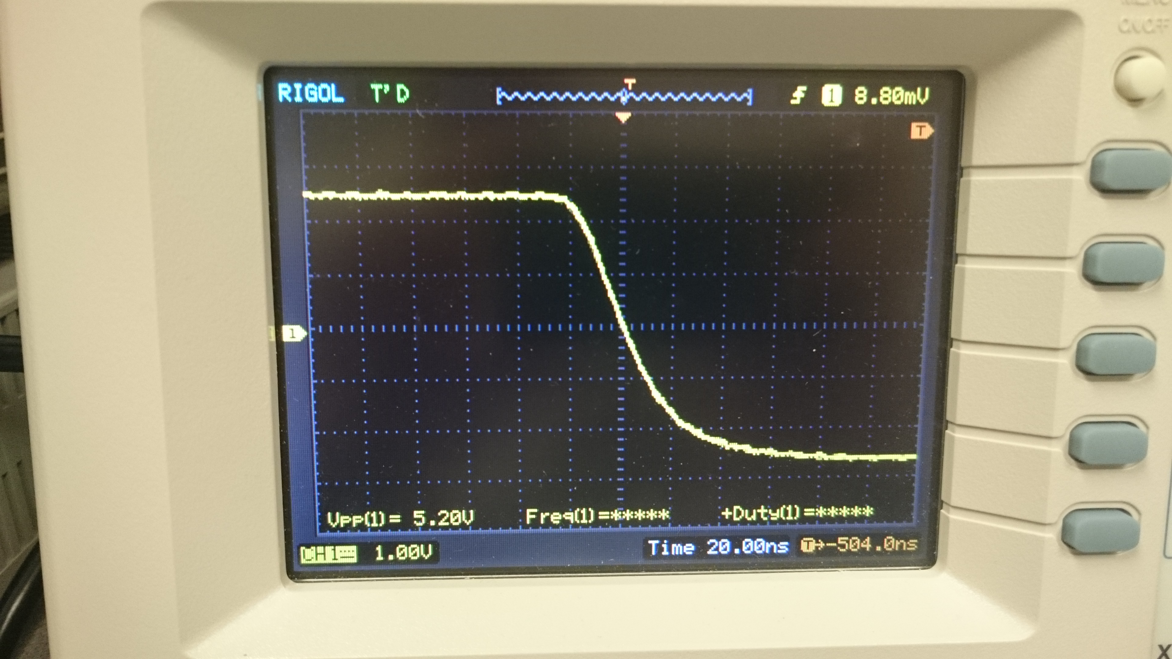
The next challenge was square waves. I was pleasantly surprised to see a decent 1MHz square waveform and even at 5MHz, it wasn’t too horrible. At frequencies much above 5MHz, the square edges were mostly gone, especially at higher voltages (see the difference between a 5vp-p square wave and 1v p-p square wave at 10MHz below); this again suggests an analog output stage limitation (op-amp with insufficient slew rate). Regardless of the amplitude setting, there was a *lot* of jitter at higher frequencies which is certainly not an output stage problem. Duty cycle control worked as expected.
FY3200S 5MHz 5V Square Wave
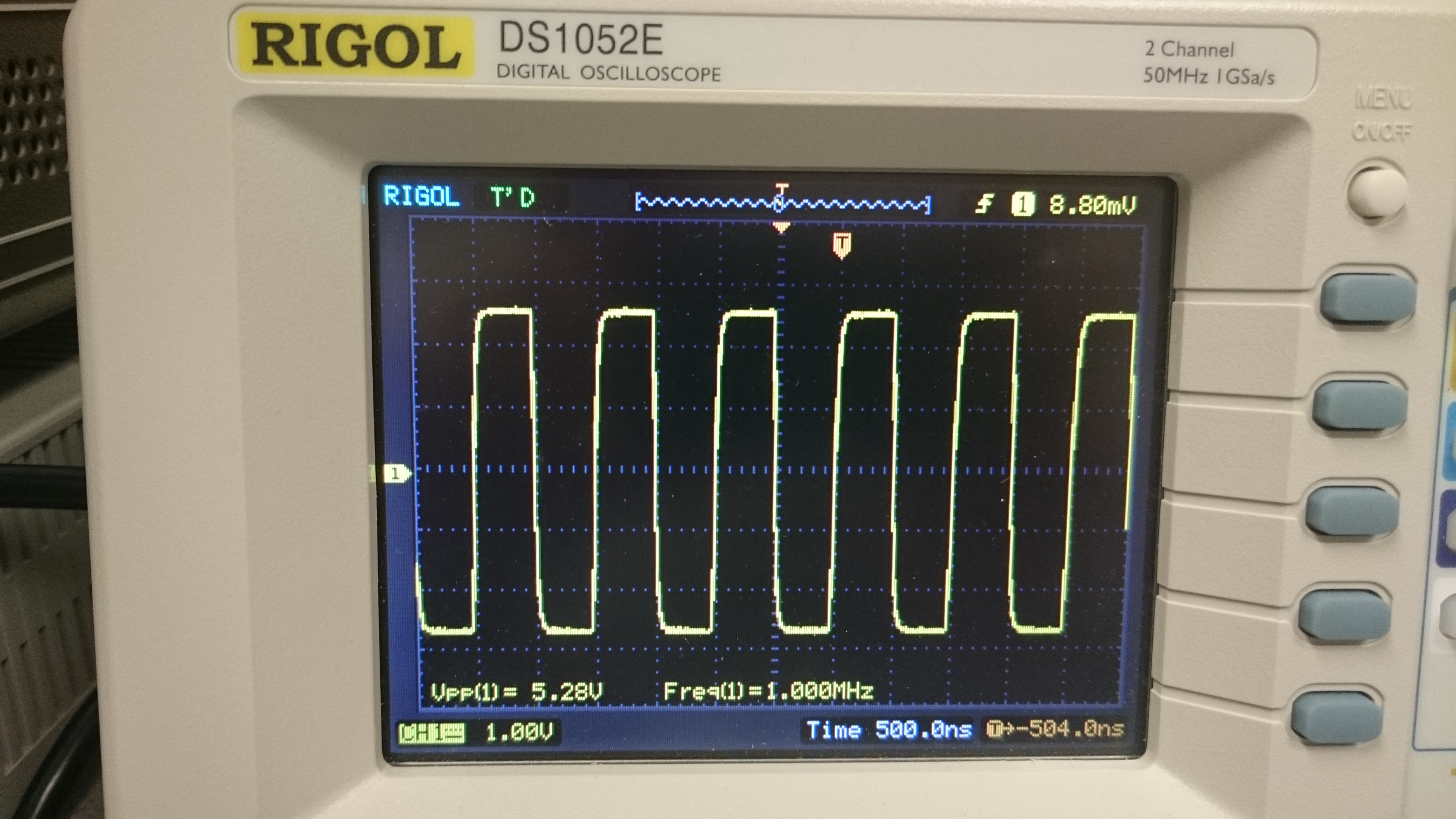
FY3200S 1MHz 5V Square Wave
FY3200S 5MHz 5V Square Wave
FY3200S 10MHz 5V Square Wave
FY3200S 10MHz 1V Square Wave Jitter
FY3200S Duty Cycle
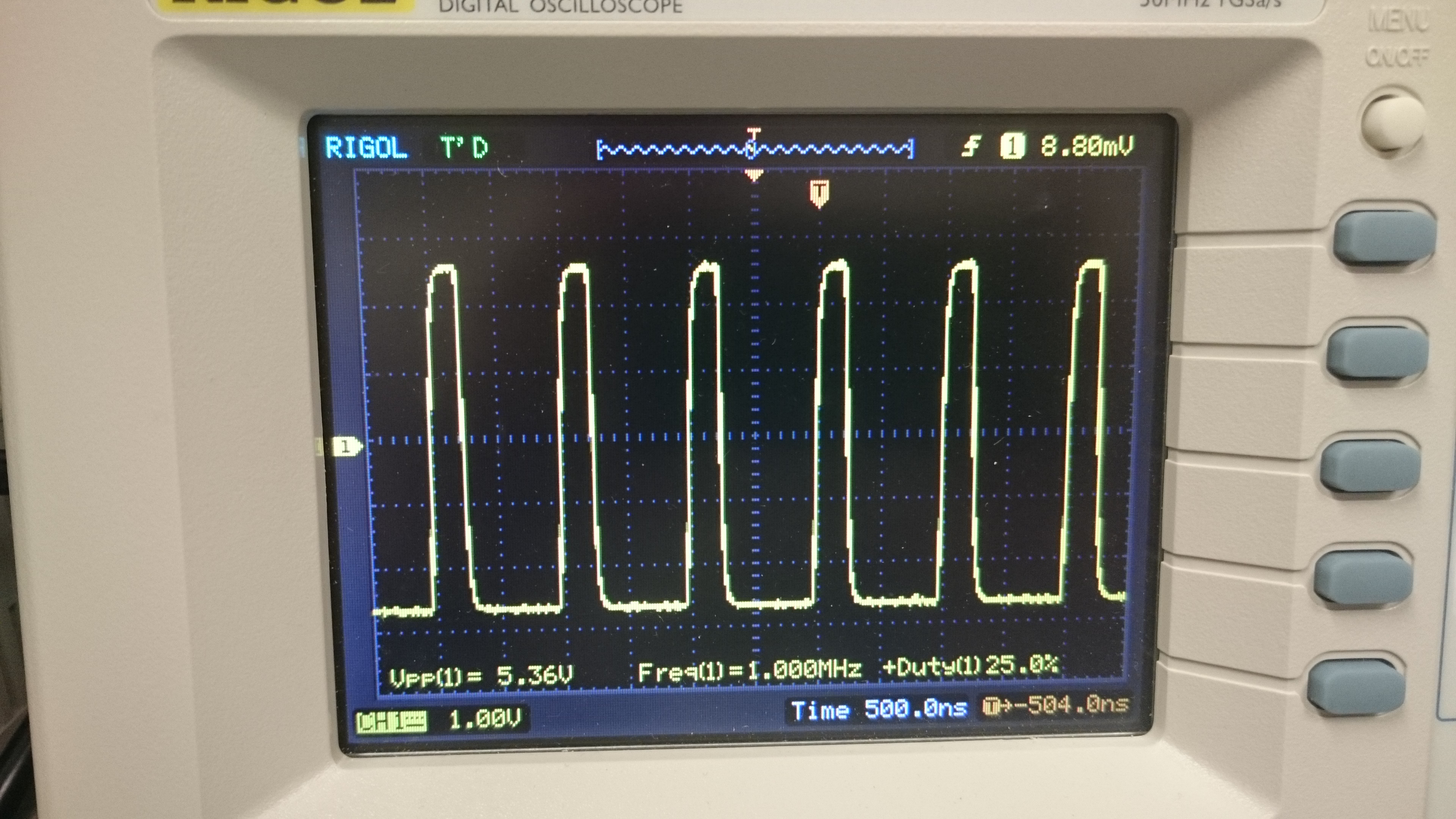
FY3200S 1MHz 5V 25% Duty Square Wave
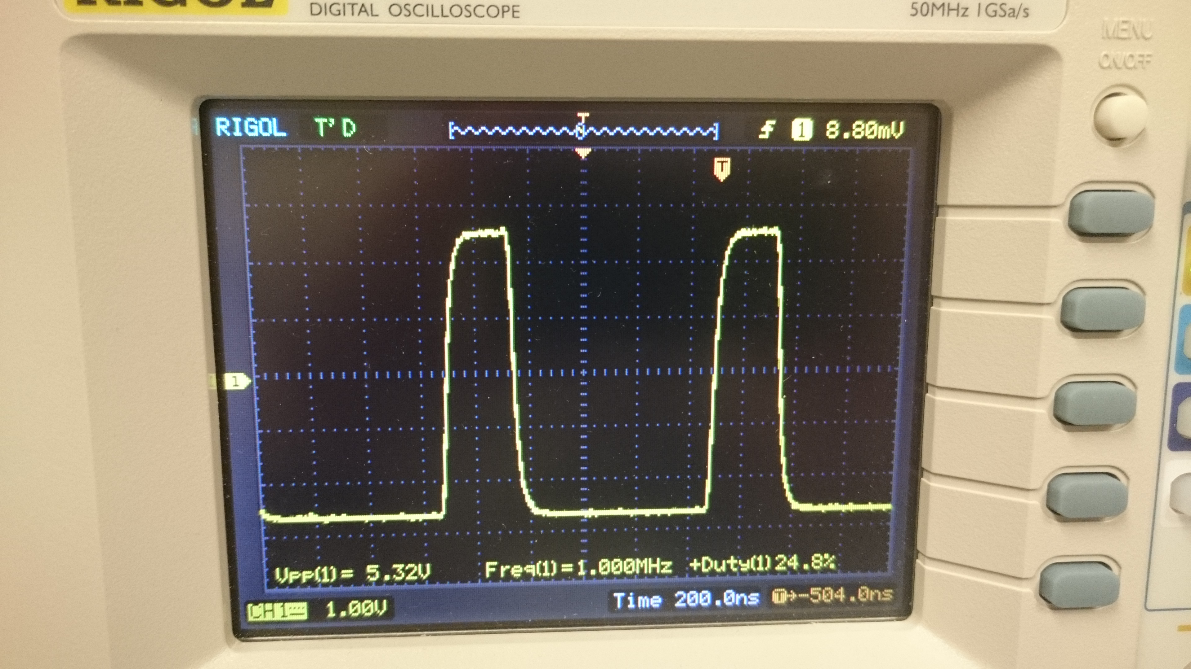
FY3200S 1MHz 5V 25% Duty Square Wave
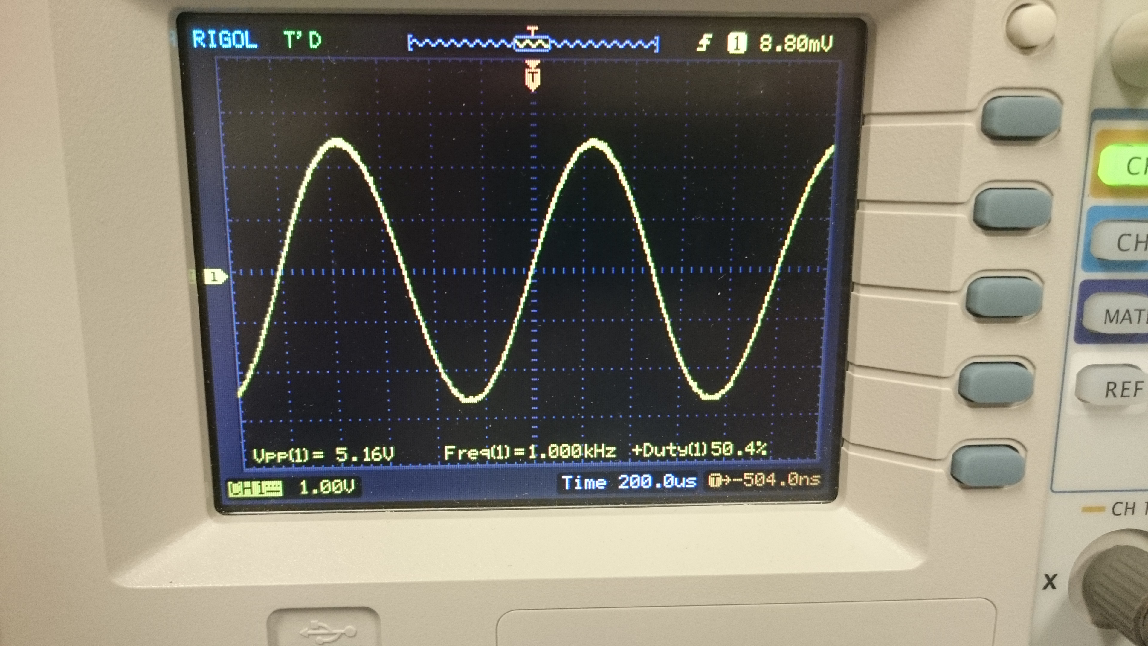
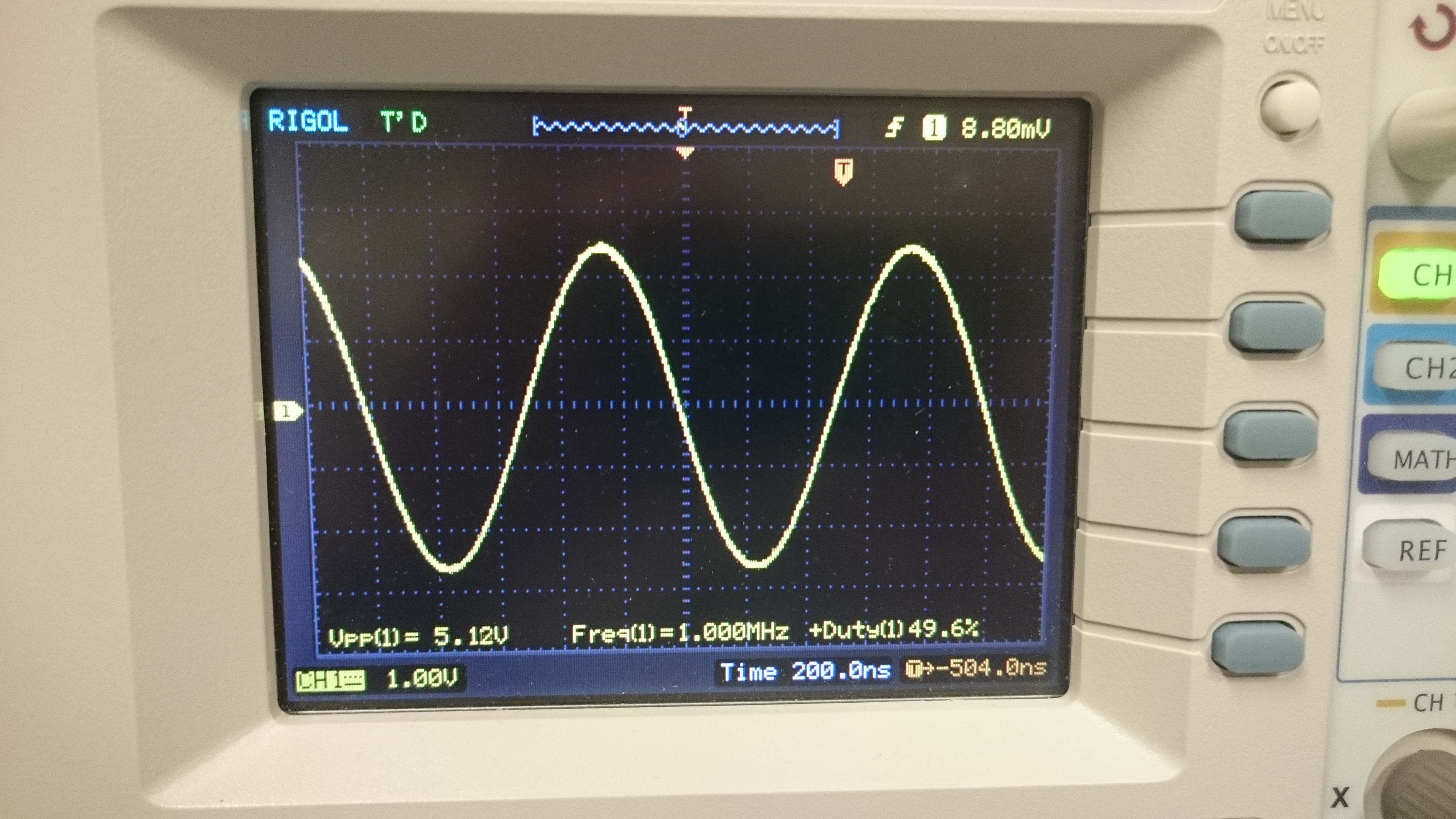
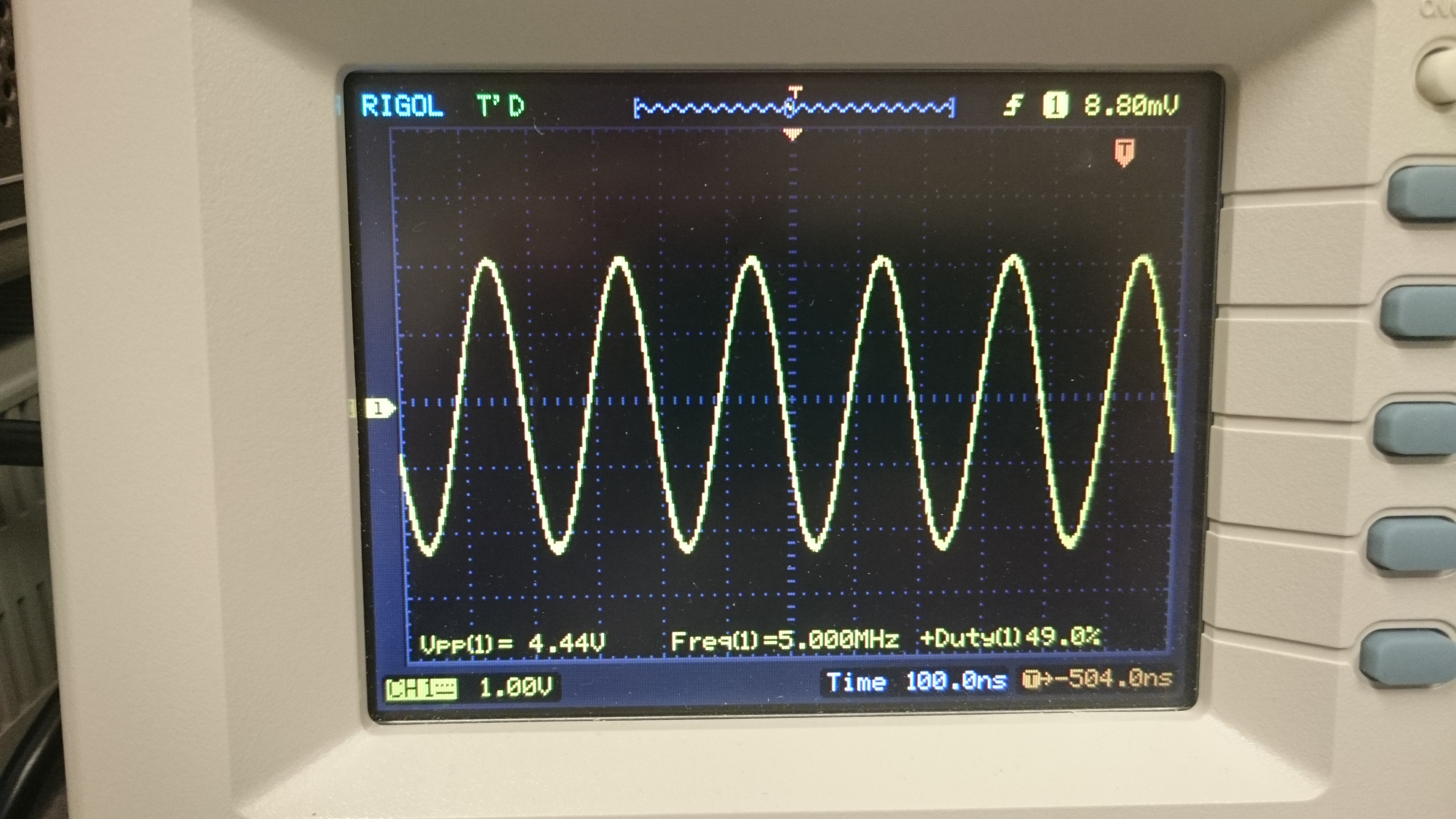
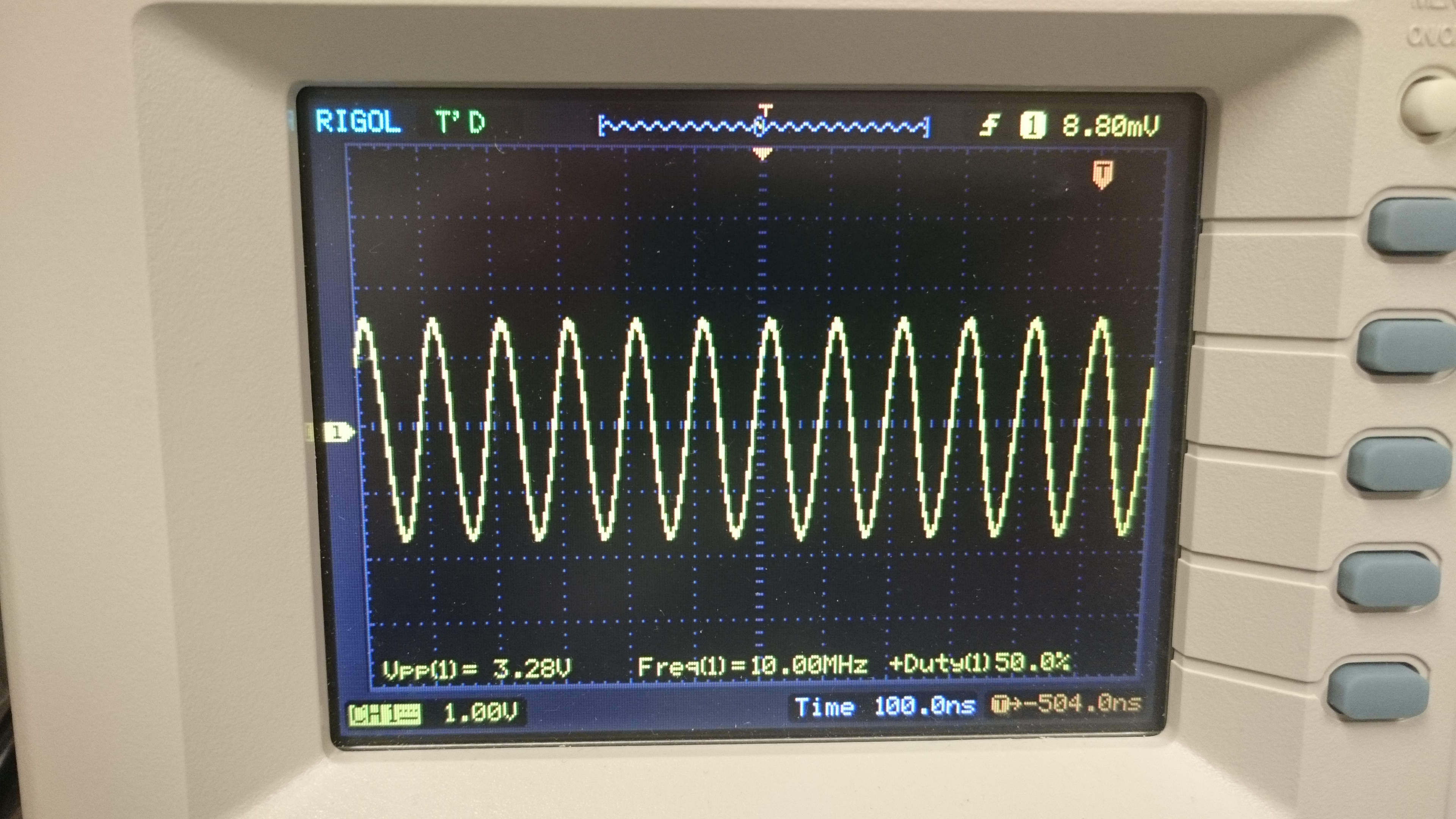
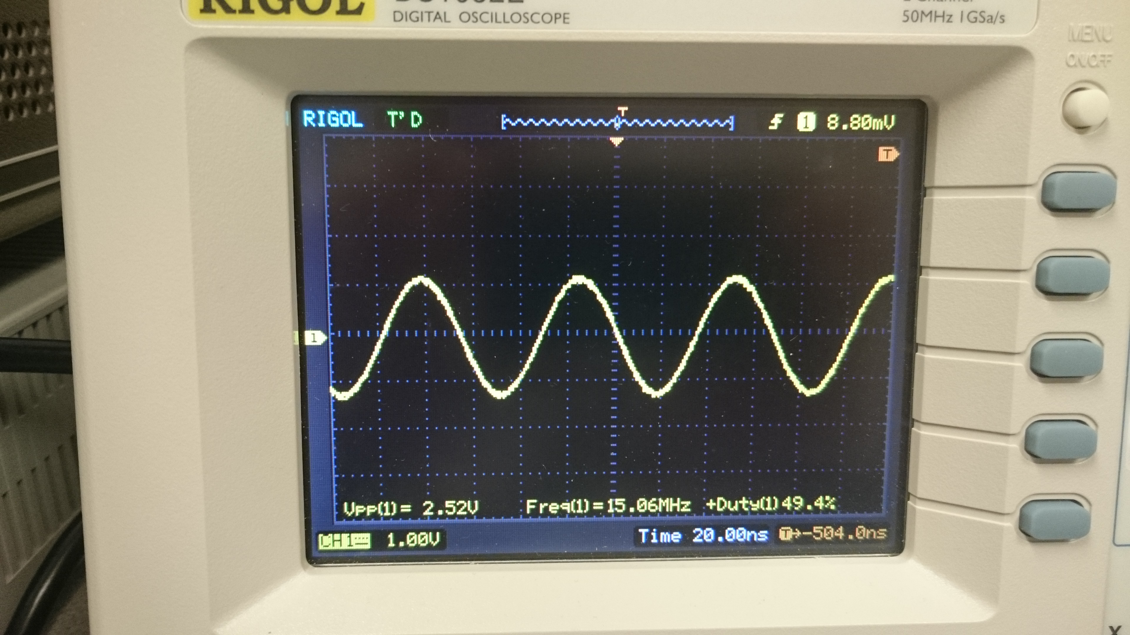
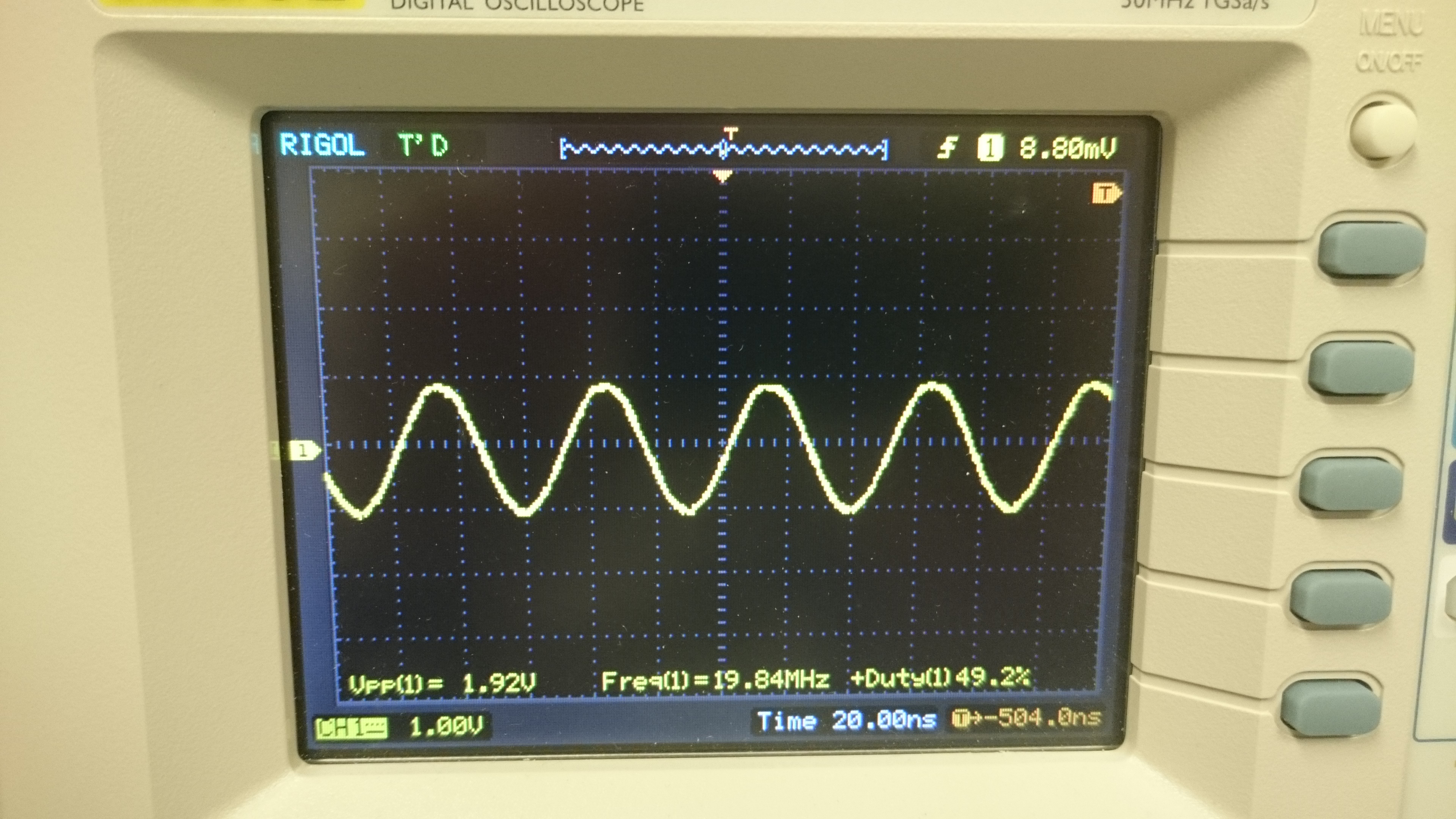
I thought it would be interesting to compare the results with a Rigol DG1022U set to generate a 5v sine wave (yes, I know I should have used a 1v sine wave).
1MHz = 5v12
5MHz = 4v44 (88% of nominal vs. FY3200S: 86%)
10MHz = 3v28 (66% vs. 59%)
15MHz = 2v52 (50% vs. 42%)
20MHz = 1v92 (38% vs. 29%)
24MHz = 1v68 (34% vs. 21%)
Rigol_DG1022U
DG1022U_1KHz_5V_Sine
DG1022U_1MHz_5V_Sine
DG1022U_5MHz_5V_Sine
DG1022U_10MHz_5V_Sine
DG1022U_15MHz_5V_Sine
DG1022U_20MHz_5V_Sine
DG1022U_24MHz_5V_Sine
DG1022U_1MHz_5V_Sqr
DG1022U_2MHz_5V_Sqr
DG1022U_5MHz_5V_Sqr
DG1022U_1MHz_Sqr_Edge
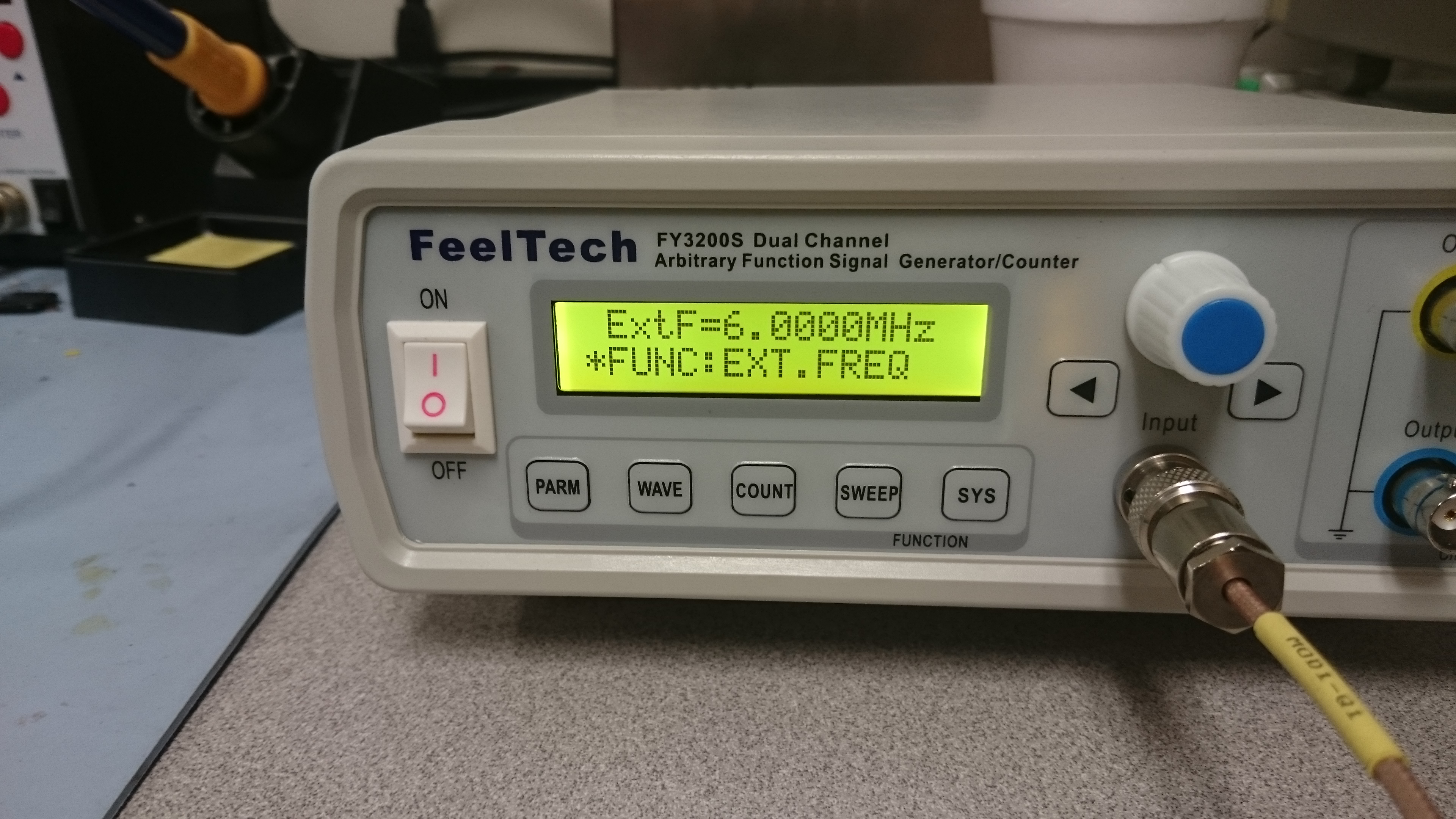
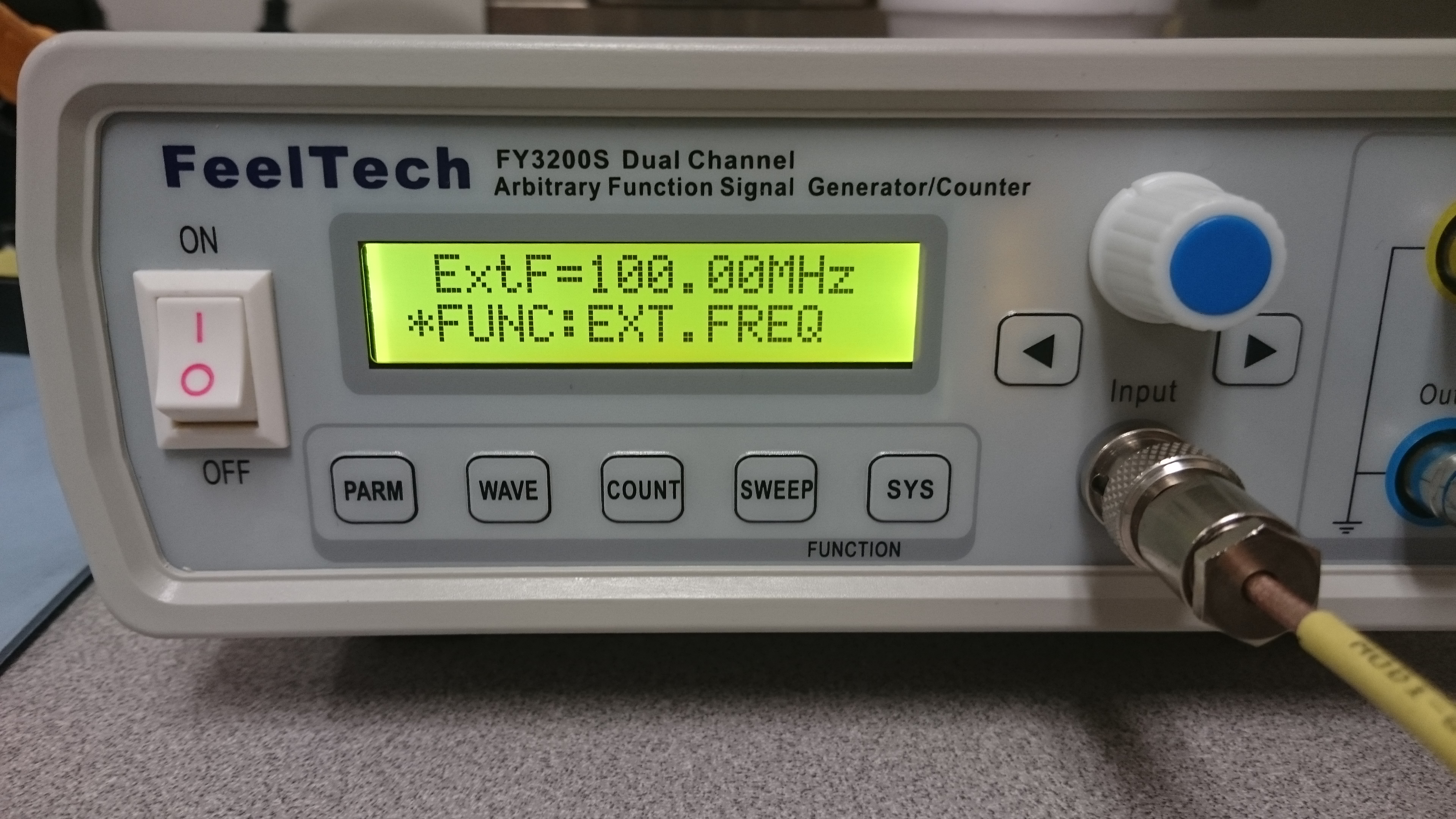
I ran several tests of the frequency counter to try to find its limits. It met the 100MHz spec at +7dBm signal strength and actually reached 225MHz at +13dBm (the limit of my generator). My source was a Marconi/IFR RF signal generator. The test results were:
-5dBm: 6MHz
0dBm: 47MHz100MHz: +7dBm
+13dBm: 225MHz
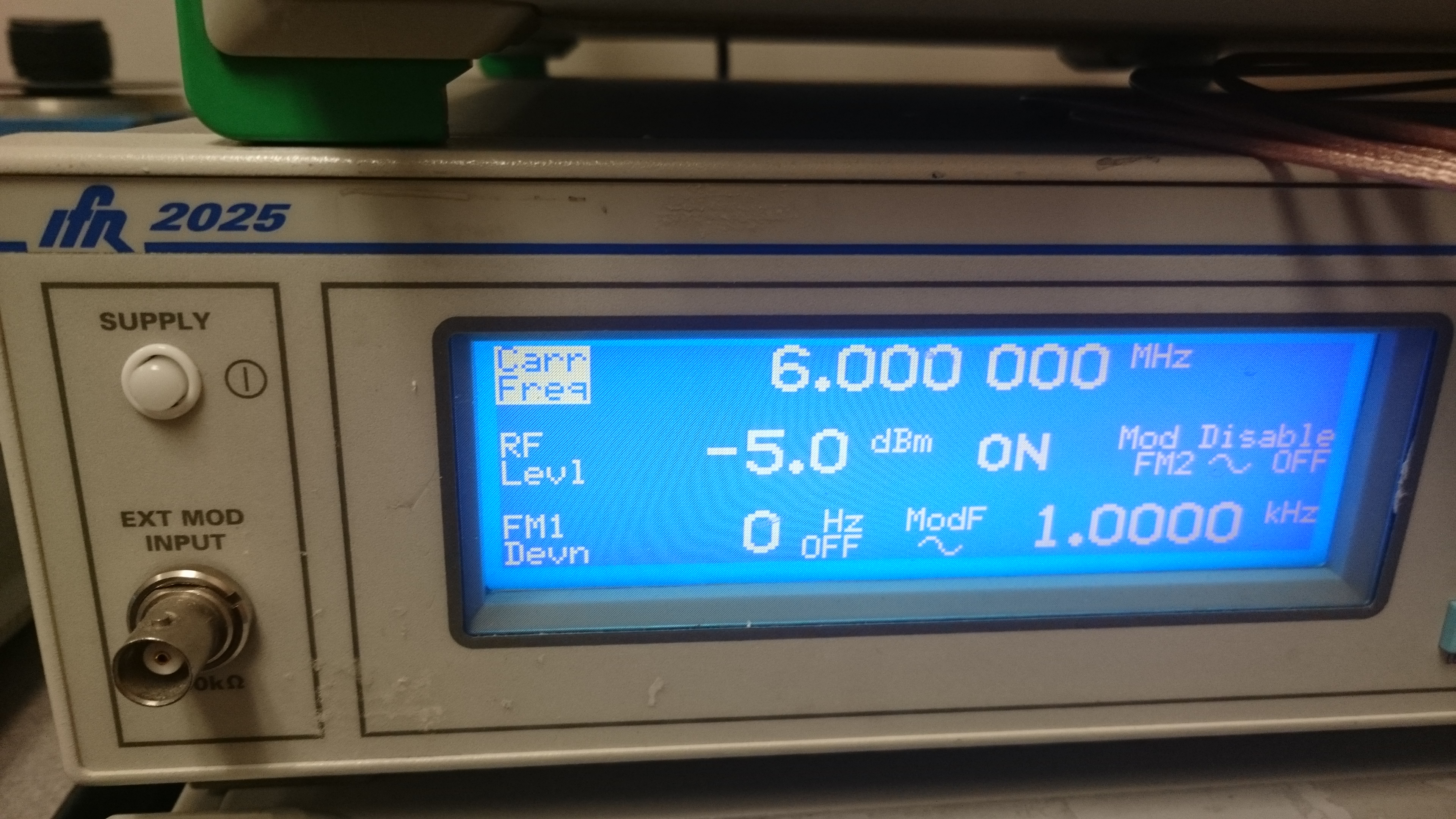
Signal Generator 6MHz
FY3200S_6MHz_Neg5dBm
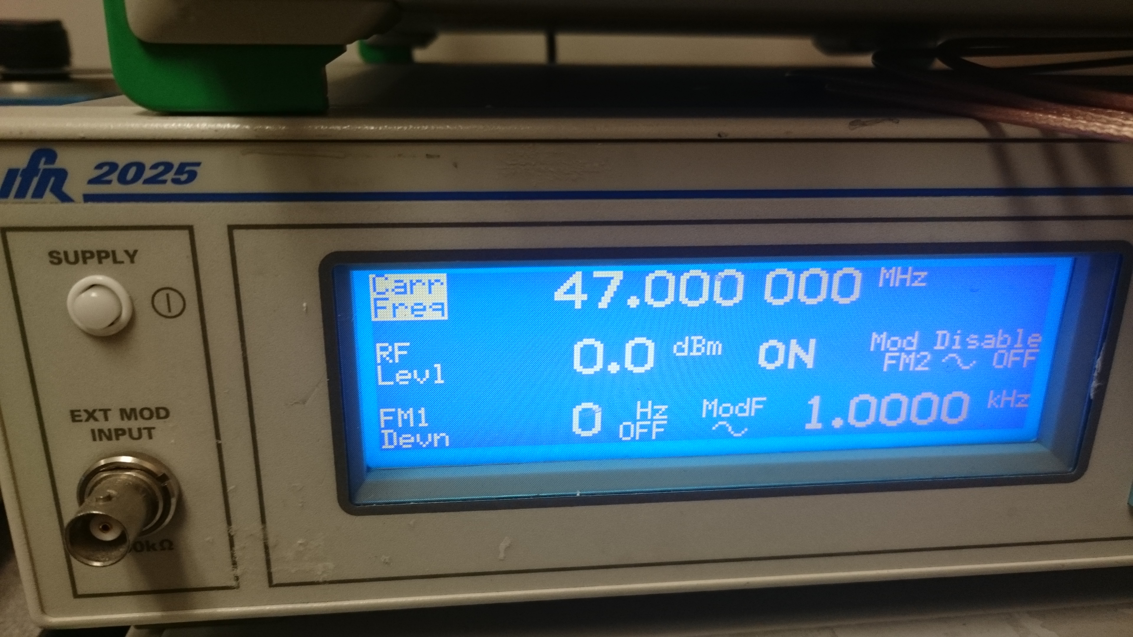
Signal Generator 47MHz
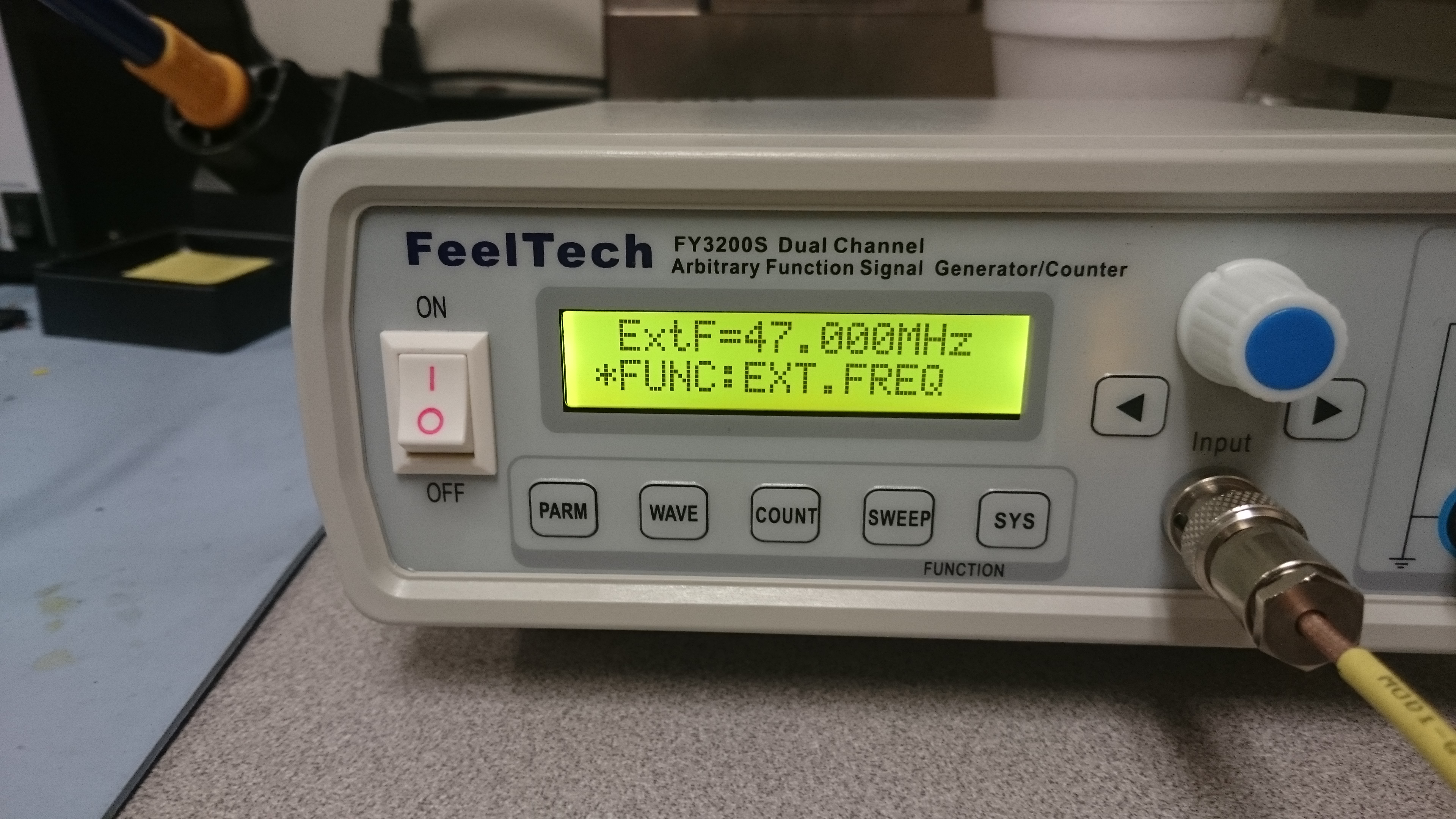
FY3200S 47MHz 0dBm
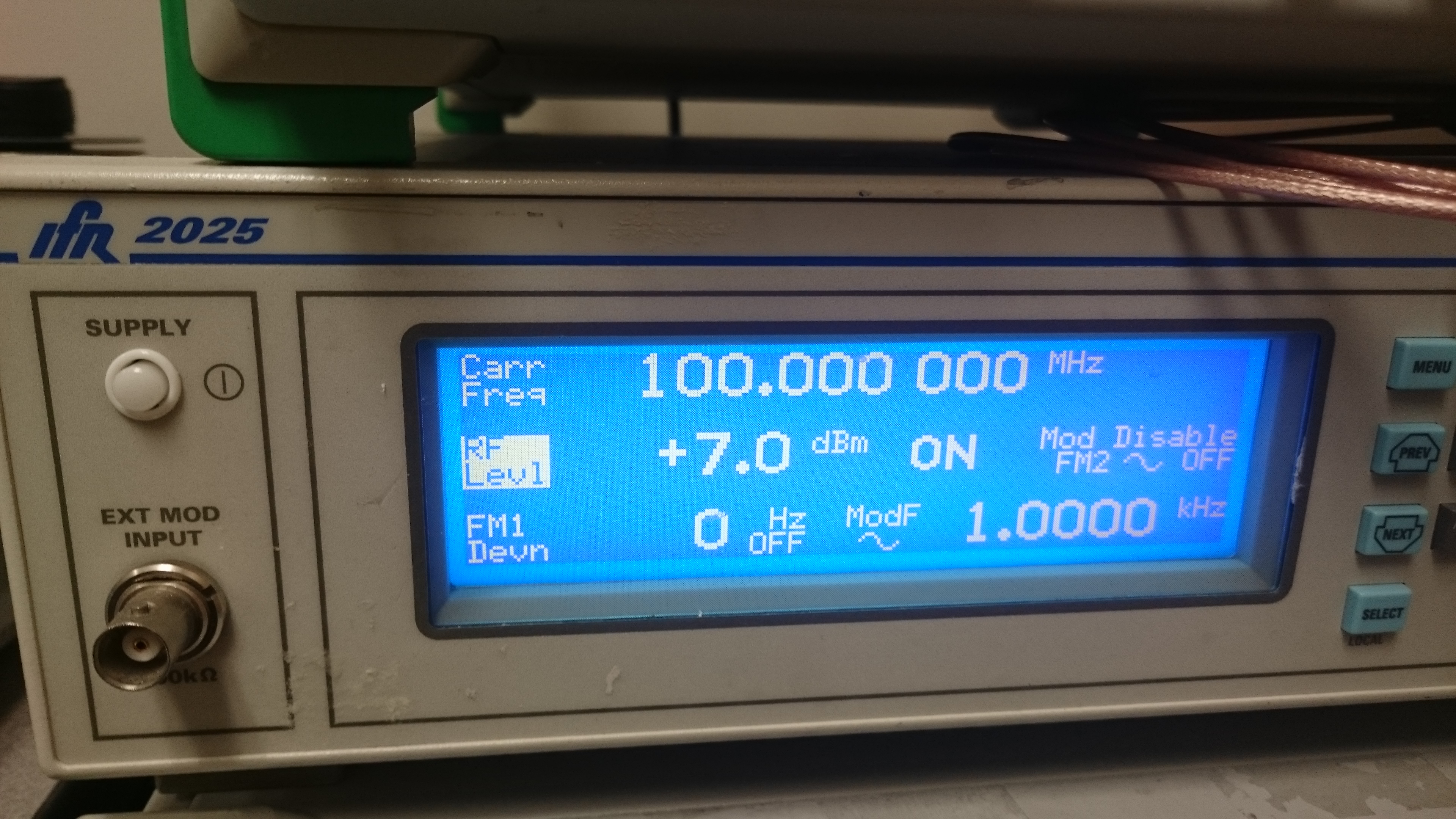
Signal Generator 100MHz
FY3200S 100MHz 7dBm
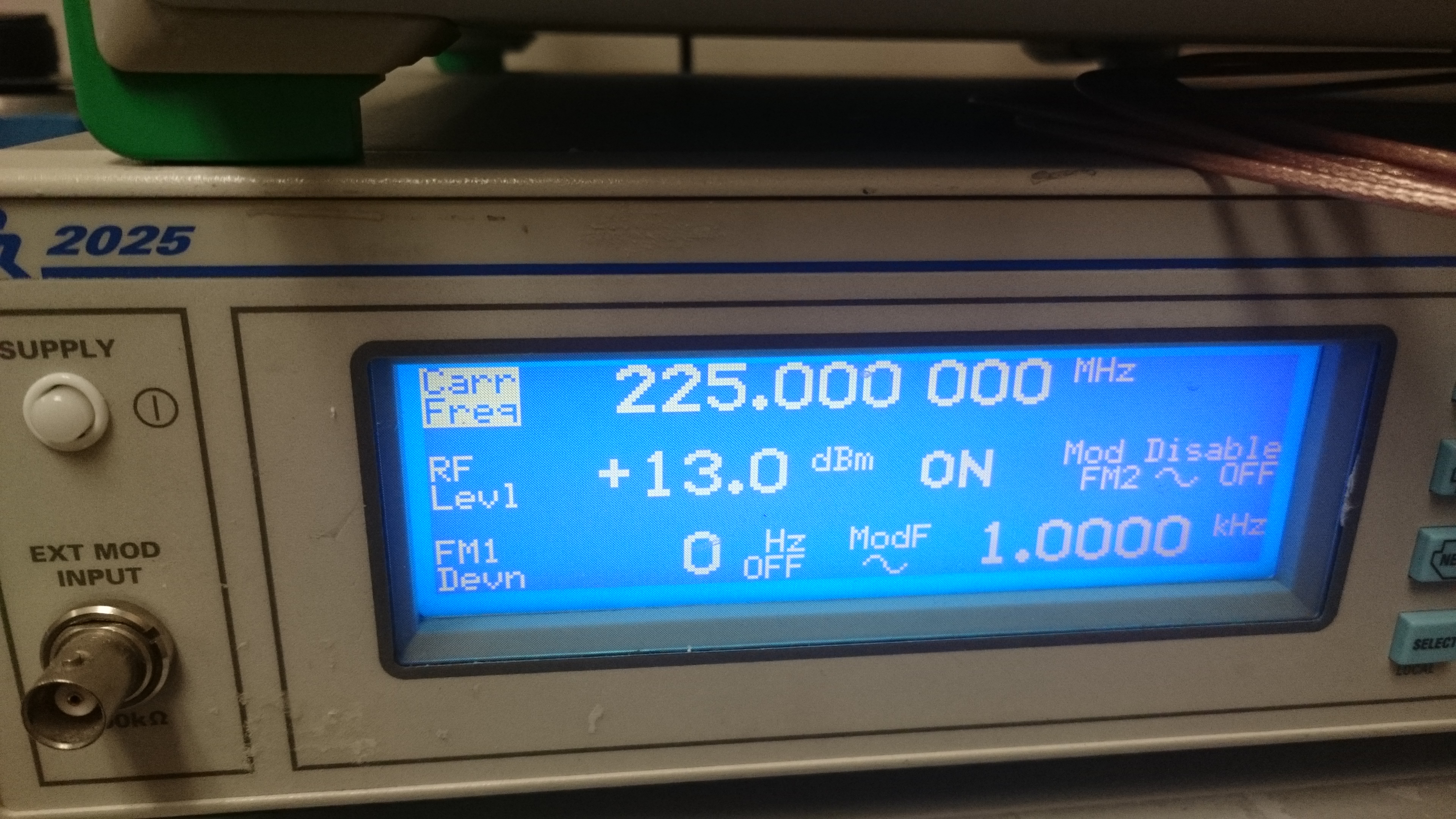
Signal Generator 225MHz
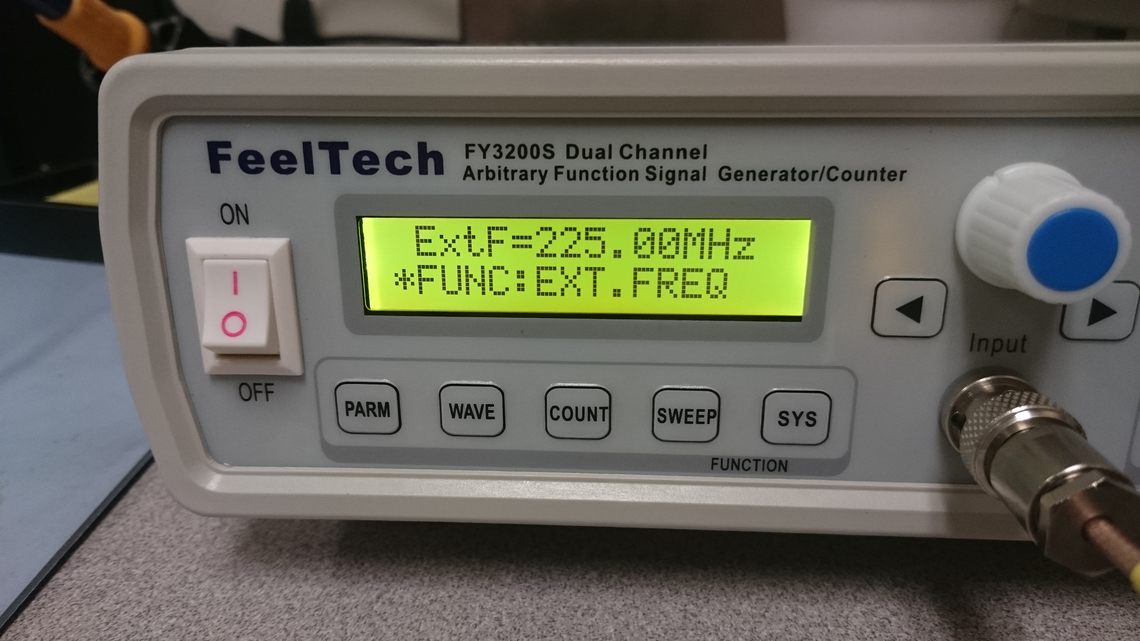
FY3200S_225MHz
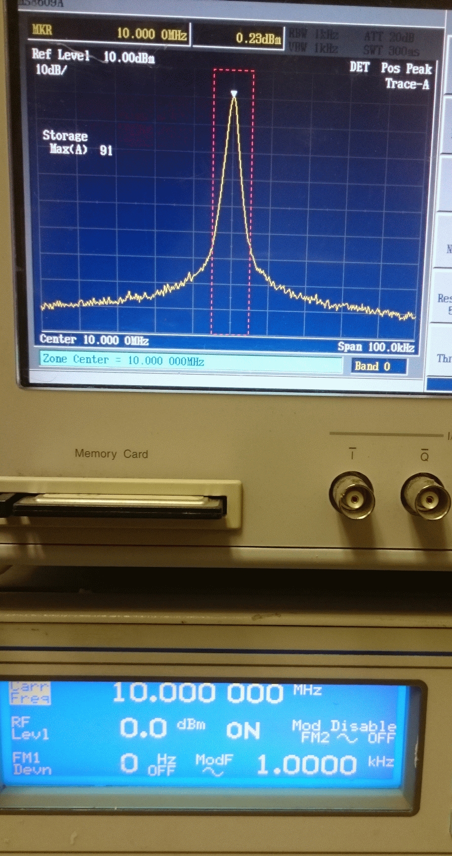
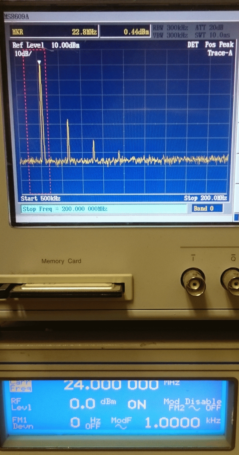
Finally I wanted to look at the spectral purity of the generator; I used an Anritsu MS8609A spectrum analyzer to examine 1V sine waves at 100kHz, 10MHz, and 24MHz. I examined close-in spurs that are typically modulation caused by noise in the power supply and harmonics to see how well the analog output filter works. I’ve also included a few pics of the output of a high quality RF signal generator (Marconi/Aeroflex IFR2025) for comparison. Overall, the Feeltech generator did better than I’d expected.
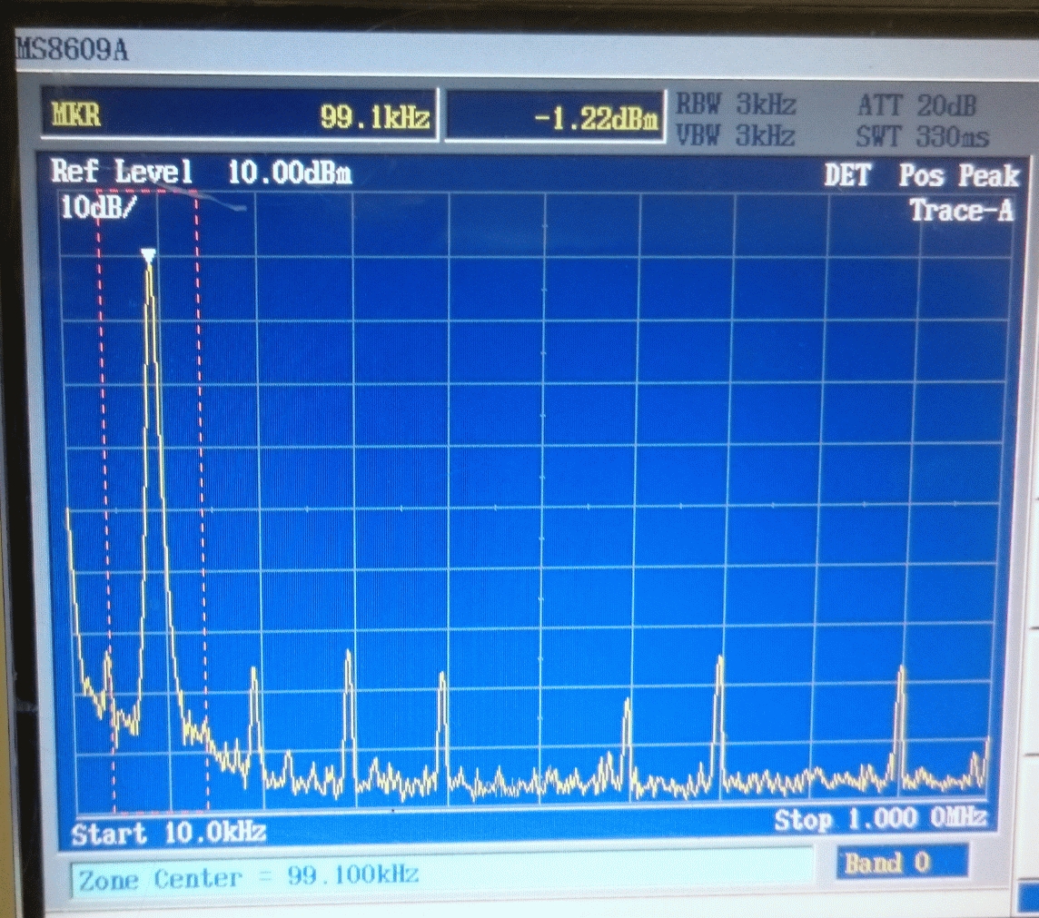
FY3200S 100kHz 1V sine harmonics
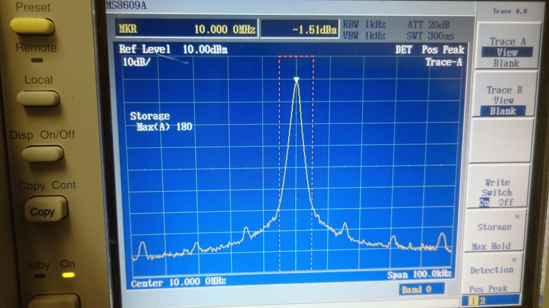
FY3200 10MHz sine spurs
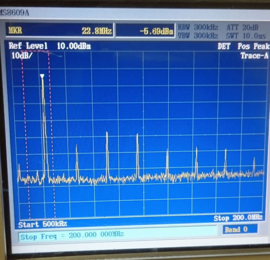
FY3200S 24MHz sine wave harmonics
IFR2025 10MHz sine spurs
IFR2025 24MHz Harmonics
My conclusion so far is that while the Feeltech it is not as good a signal generator as the Rigol (no big surprise here…it’s less than 1/4 the cost), but in terms of output quality and capabilities, it comes pretty close and for many applications, it is quite usable and appears to be an excellent value. The frequency counter is a nice bonus!
If time permits, I’ll tear it down and look at the output stage and timebase to see if any improvements can be made.
Owon VDS1022
I recently purchased an Owon VDS1022 USB oscilloscope (two of them actually). I’ve wanted a USB oscilloscope on my desk for a long time. A USB scope *should* be much less expensive than a bench scope since it relies on the PC for its user interface and processing power, however I’ve tried several low-cost USB scopes and they have been disastrously bad due to low sample rates and awful software.
I ordered the Owon VDS1022 from Amazon for $80 shipped or $108 for the isolated version. After some initial tests, it looks pretty good! It’s main constraint is the 100MS/s sample rate, however if you can live within that bandwidth constraint it does quite a good job. I fed it sine waves up to 25MHz from my signal generator and it reproduced them faithfully. Square waves are, of course, tougher since they contain so many (infinite) high frequency components, but up to 5MHz it is very good and even at 16MHz, it does a decent job. At 16MHz, you’re only sampling ~6 points per cycle so the waveform displayed may be greatly smoothed with higher frequency details lost (for example, you won’t see sharp edges or higher frequency ringing), but it is still good enough for many of my needs.
The enclosure is aluminum and looks and feels solid and high quality as does the USB cable and the two included probes (although the probes are only rated for 6MHz at 1x and 60MHz at 10x). The rubber bumpers on the end are probably good for portable use; they can be removed and the silkscreen is duplicated underneath.
The software is very nice. It installs perfectly on Windows 7. On Windows 10, it was another story; eventually I figured out that after installing the software, you need to plug the scope in and install the driver manually from the Windows Device Manager (find the scope in the device manager and then update the driver (which in my case was in C:\Program Files (x86)\OWON\VDS_C2\USBDRV), once you have the driver installed, the software works well on Windows 10. Sadly, the software doesn’t work at all on Linux, even under Wine; the issue is the USB driver. The software is intuitive, fast, and the interface is clean; I never had to refer to the manual. It measures frequency automatically and they’ve added keyboard shortcuts for some of the most common operations (vertical and horizontal scales up/dn) which are *very* handy…I wish they would add a few more keyboard shortcuts, especially run/stop, single-shot re-trigger, and vertical position. The software includes an extensive set of automatic measurements under the Math settings including spectrum analysis (FFT); on the big PC screen you can have many measurements active without cluttering the display.
At this price, the VD1022 seems to hit the right price-point for its feature set; it’s a no-brainer to choose it over the Hantek or SainSmart low-end USB scopes. If OWON drops the price a bit on their faster USB scopes, I’ll probably buy one of those too.
Update: 12/8/2015: I was curious to see if the non-isolated scopes could be upgraded and sure enough, remove 8 resistors and install two ICs for power and signal isolation (U37: ADUM3160BRWZ-RLCT, U9?: DCP20505U) and the scope works and is isolated (at least no DC connectivity)…the cost was just under $40 for two scopes ($20 each).
Update: 7/8/2016: I like these VDS scopes so much that I bought a VDS2064 (60MHz, 4 channel, LAN interface). I haven’t figured out the LAN interface yet, but I can confirm that it works nicely over USB with Windows 10 (requires the same manual process for installing the USB driver described above). I now have a VDS on my work office desk, home office desk, and in my robotics backpack. After purchasing these USB scopes, I haven’t turned on my traditional bench scopes except once to look at a VHF signal (had to use my old 500MHz 5GS/s Tek scope).
Owon needs to start making more USB-connected test gear (signal generator, logic analyzer, etc.) in this form factor!
ZTW 7×7 CNC machine
After reading a bunch of positive reviews, I purchased a Zen Toolworks 7×7 CNC machine on eBay. It came with three SST43D2121 stepper motors, a 3-axis Univelop TB6560v2 motor controller , and a spindle (high speed 36v milling motor). There is a remarkable absence of documentation for this stuff on the internet…hopefully this blog post will help.
I purchased a a MeanWell model S-100F-12 12v power supply ($20 on eBay) that supplies 12V/8.5A and connected it to the +7, +12v, GND inputs on the motor controller; numerous posts indicated that the 7v input can take 12v and so far I’ve had no problems with that.
The wiring to the stepper motors is just as described on ZTW’s website:
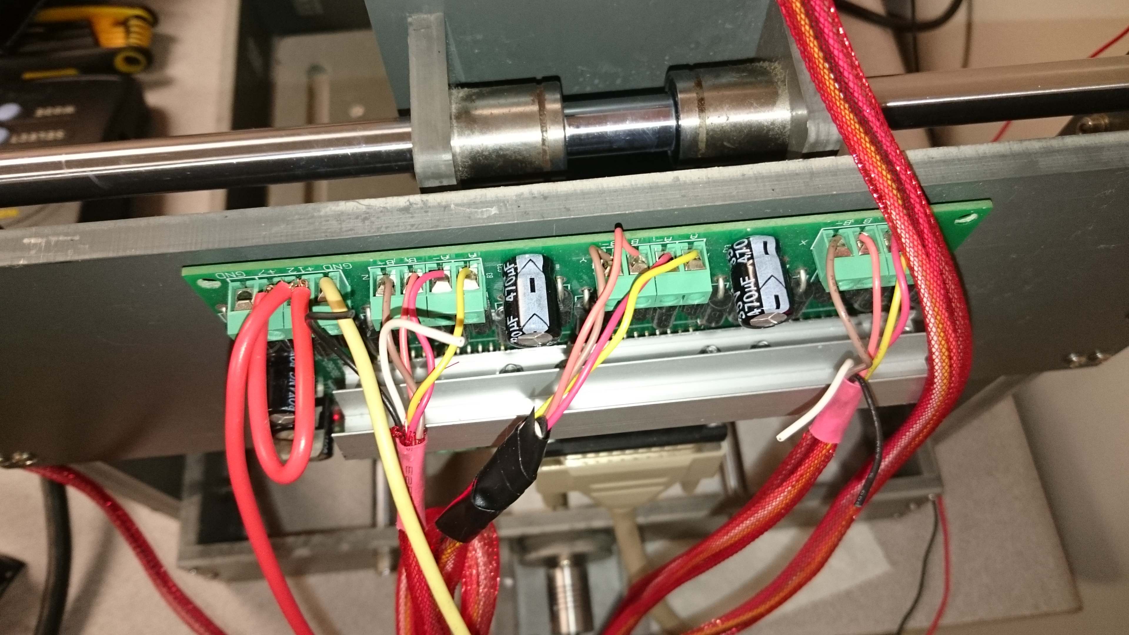
Stepper motor wiring
The motor controller has two sets of DIP switches for each motor: one has 2 switches and the other has 4 switches. On the 2x switches I set 1,2=ON. On the 4x switches I set 1=ON and 2,3,4=OFF.
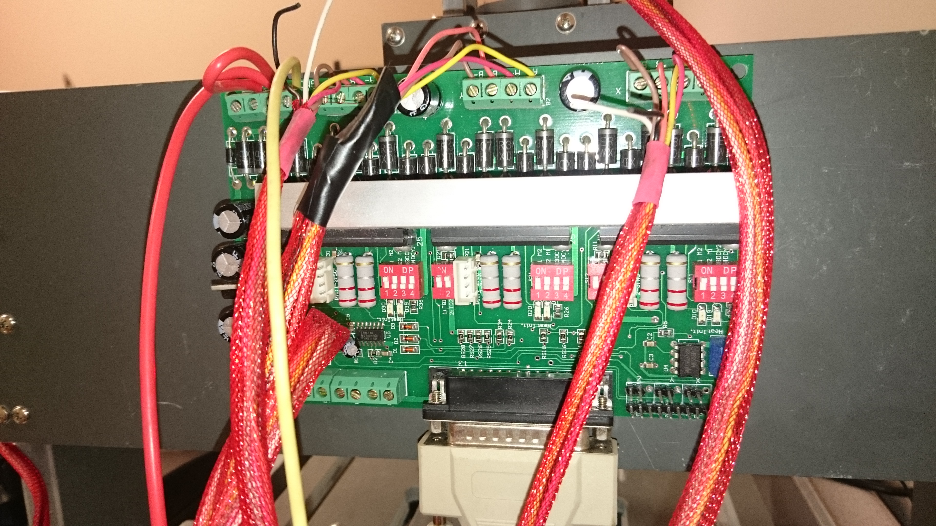
DIP Switches
This configures the motors for minimum (20%) current and smoothest movement (1/16 microsteps, 0% decay). This was determined by trial and error. Using the lowest load setting was important because the software I’m using (LinuxCNC) turns the motors on when powered; they are either held locked in place or driven (moving) but never turned off; so they are constantly drawing power…with 20% current, they stay cool and the 12v supply is never drawing more than 9.x Watts for all 3 motors and the controller. Using the 1/16 microsteps made a huge difference in smoothness of movement; otherwise moving the motors was very noisy.
The motor controller connects to the computer using a straight-through DB-25 cable. The pins are used as follows:
2 = Out = Step X
3 = Out = Dir X
4 = Out = Step Y
5 = Out = Dir Y
6 = Out = Step Z
7 = Out = Dir Z
8 = Out = Enable Y
9 = Out = Enable Z
14 = Out = Enable X
10 = In = Emergency Stop (low***)
11 = In = Limit X (low***)
12 = In = Limit Y (low***)
13 = In = Limit Z (low***)
1,15,16,17 = N/A = Not Utilized
18-25 = GND
***Signals are Active Low
Note that the Enable line must be active (high) for a motor to turn. When properly configured, the software will enable the motor when the machine is powered and disable the motor when the emergency stop button is pressed (in software or hardware) which powers-down the motors.
I’m using LinuxCNC for the control software; it’s free and I like linux. You can read about it here. The software is extremely configurable which makes figuring the setup out problematic. The software comes with two configuration wizards; one is for stepper-motor-based machines. I used this and created a configuration file named ztw7x7, but the wizard doesn’t allow you to configure the Enable pins properly. In the end, I had to edit the .hal file by hand to add definitions for Xenable, Yenable, and Zenable. This link was very helpful. I’ll post the edited file shortly.
There are many good choices for controlling NEMA17 stepper motors (1.2A/phase) including Arduino (Uno or Mega2560) with GRBL software (optimized for Mega2560 here) with a CNC shield using the Allegro A4988 or TI DRV8255 drivers (1-2A w/fan) or TB6600 stepper motor drivers (3.5A). See install info here. Note that the drivers must be adjusted for max current and many suggest adding over-voltage protection for them including a 100uF cap across the motor. I would consider a suitably sized TVS diode instead because most 100uF caps aren’t rated for the ripple current they would experience.
Replacement spindles are available with 775 motors and the same ER11 spindle.
DIY PCB single-sided success
I am finally having success making single-sided PCBs at home using the toner transfer process. I am generally using traces no thinner than 12 mils (although I think I did 10 mils a few times and it worked fine) and 12-15 mil spacing. With modern surface-mount parts, it’s amazing how much of the circuit can be done in a single layer and without drilling.
I’m using products from PulsarFx that are specifically made for this process and they work much better. I came tantalizingly close many times using McGyver methods (magazine paper, clothes iron, etc.), but it never worked quite right and cost many hours of frustration. In particular, getting the paper to release from the toner was always a problem and I often experienced over-etching. I tried magazine, matte, and many varieties of glossy paper from Staples. In the end, the PulsarFx products are not that expensive and work perfectly.
I have no relationship with PulsarFx other than that I am a customer and am now a fan.
The current process:
- Print on PulsarFx toner transfer paper using an HP 1025nw printer. Printing did not work well with my Canon D420 printer (did not put enough toner down) and I couldn’t feed the thick transfer paper through my Samsung ML-1865W or ML-2160. The transfer paper is coated with a material that dissolves quickly in water, so after the toner is transferred to the copper board, the paper releases perfectly every time. Configure your printer for thick glossy paper, black or grayscale, and maximum toner output.
- Clean a blank copper board to a bright shine using steel wool. I get the blank copper-clad boards on eBay from seller abcfab; ideally you should use 1/2oz copper for much faster etching, but I’ve also had success etching 1oz and 2oz copper. After cleaning with steel wool, I’ve tried using tarn-x and/or acetone and they may help slightly but I’ve had good results without them. Once the board is bright and shiny everywhere, don’t touch it with your bare hands…use gloves to avoid getting skin oil on it. I use nitrile disposable gloves throughout this process; they cost $8 for 100 at Harbor Freight Tools.
- Place the printed pattern face down (toner touching the shiny copper) on the copper board and run it several times (like 10) through a laminator. I am using the PulsarFx “Applicator” which is just a big laminator. I also have a much cheaper Harbor Freight Tools laminator which I am going to try and report on. The board gets hot after a few passes through the laminator so I use leather work gloves.
- After lamination, soak the board with the transfer paper stuck to it in water, I use a plastic tupperware container. After a minute or two (sometimes within seconds), the paper’s coating dissolves and the paper just floats away from the copper board leaving the toner pattern on the copper. Throw away the paper and pat the board dry with a paper towel. The water and container gets used again later in this process so keep it handy.
- Follow the directions on the package and cut a sheet of PulsarFx Green Toner Reactive Foil a little larger than the copper board (2″ longer). Place the foil dull-side down on the board and wrap 2″ under the board. Place the side with the board with the 2″ wrapped under it in the laminator and try to keep apply some drag to the foil with your fingers as it goes through the laminator to prevent the foil from wrinkling. I don’t have this quite right yet, but it still works pretty well. I put it through the laminator a second time to make sure it has stuck. Then peel the foil back from the board at a 180-degree angle. What’s left is green foil covering most if not all of the toner. The foil creates a stronger barrier to the etchant; without it, the etchant sometimes eats through the toner in places before the etching is finished resulting in pitting or uneven edges. With the foil, I get perfect etching and nice clean edges, even with 2oz copper on the boards.
- In another plastic (e.g. tupperware) container, mix the etching solution using nitrile gloves and chemical protective glasses, and preferably wearing old clothes: pour 1 cup of hydogen peroxide (purchased at my local supermarket) into the tupperware then mix in 1 cup of muriatic acid (hydrochloric acid) which I get in 1 gallon containers from Lowes which costs around $5/gallon. I use a disposable styrofoam coffee cup as a measuring cup. Because this is a sadly litigious world: these are harsh chemicals; don’t get them on your skin, on your clothes, or in your eyes; it is acid, it’s dangerous. Use proper protective gear, if you don’t know how to handle chemicals, don’t do this. Proceed at your own risk. I do this in the back yard because the fumes (and liquid) can be corrosive to nearby metals. I am going to try this again with the white vinegar/peroxide/salt etching method and report back.
- Place the copper board in the etching solution with the pattern facing up; every minute or two gently brush the surface of the board with a foam paint brush (around $0.79 from Lowes). Brush it a few times to brush away the etched material and expose more shiny copper; this makes the etching process go much faster.
- When the copper is all gone and only the toner/transfer foil is showing, remove the board from the etchant and place it in the other tupperware container containing just water to stop the etching. Note: the etchant solution doesn’t seem to effect the nitrile gloves so I just take it out by hand.
- Carefully (gloves, chemical glasses) pour the etchant into a plastic container for storage and/or disposal. I use a plastic funnel and a plastic bottle that seals liquid tight (e.g. an iced tea or juice bottle). Take your time doing this so nothing splashes out. Seal the bottle, then rinse clean your brush, tupperware, circuit board, etc. You can’t just pour the used etchant down the drain (it is toxic and will probably ruin your pipes). Take it to your local recycling/waste disposal facility for proper disposal (I’m looking into ways to manage this better).
- The final step (for me, for now) is to remove the toner and foil from the board. This is done using a rag or paper towel and acetone (which also costs around $5/gallon at Lowes). Do this outside too, acetone is very smelly.
When you are done, you will have a nice shiny PCB ready to solder (or drill if you are still using through-hole parts). Total time is under 30 minutes.
- For drilling, I use an old Dremel model 380 rotary tool and an old Dremel model 210 drill press (purchased on eBay for ~$20 shipped – they are commonly available there – note, this press only fits tool models 245, 250, 260, 270, 280, 350, 370, and 380). I’ve read that the 210 press is much more precise than the newer ones but I can’t confirm that. I can confirm that this combination drills precise holes in the PCB. I get carbide drill bits that fit the rotary tool from Harbor Freight Tools. You can also get them from All Electronics or Ebay.
My next steps are to experiment with soldermask, silkscreen, photo-transfer, and multiple layers. I’m also going to look into more environmentally friendly etchants or good ways to make the left over etchant non-toxic.
No more HP printers for me…
I’ve been grappling with HP’s CP1025nw printer for over a year and have concluded that HP is no longer capable of making a decent printer. This is sad because HP used to be the premier printer company. I’ve been buying HP lasers for a very long time; I had an HP Laserjet Plus back in the 1980s when they cost a fortune, but after several dismal HP printers over the last 5 years, I will no longer purchase from them.
I bought this particular color laser printer mainly for its “network” feature. Unfortunately, it seems to disconnect from the network whenever it goes into power save mode and requires manual power cycling to re-connect. When disconnected it cannot be awakened or accessed by ping, http, or any other protocol. I have tried wired and wireless connections, static and dynamic IPs…no luck. Many others have reported the same problem on multiple HP printer models.
Aggravating this is HP’s “technical support” whose goal seems to be to dissuade you from calling by repeatedly engaging in massive time-wasting exercises designed to help you understand how thoroughly ignorant they are of IP networking basics. This too is sad as it reflects a change in many technology companies: they no longer attempt to reduce support costs by improving documentation and product quality but instead focus on reducing support costs and quality by outsourcing to folks who have little connection to or interest in their company or products.
On the plus side, I’ve had great experiences with Canon laser printers for the last several years and their supplies are cheaper too!
DIY PCBs
Although I’m a big fan of PCB-Pool, I’m trying to learn to make simple printed circuit boards at home instead of having to send out (and wait days or weeks). I’m attempting the toner-transfer method now; I don’t have it quite right yet, but it seems doable…with the right process. It sounds great in concept:
- Print the a mirror image of the pattern to be etched using a laser printer on suitable paper
- Transfer the toner image from the paper to a blank copper clad PCB using heat and pressure (iron-on)
- Etch the PCB with the toner acting as resist
- Use acetone to remove the toner leaving the desired copper pattern
- Optionally tin plate
- Drill and mount components!
So far, my main obstacle has been clean and heavy toner transfer. I’ve been able to transfer some fairly fine patterns (15 mil lines with 15 mil spacing), but invariably some of the toner doesn’t transfer and then touch-ups are required. Also, the toner appears to have some holes in it which results in pitting during etching. Using sharpie to touch up the toner seems to help a bit, but the sharpie often is removed in the etching process.
- Pages from a regular magazine (e.g. IEEE spectrum) that are thin and glossy seem to work better than expensive thick glossy paper. The toner transfers onto the page and the page releases it onto the circuit board fairly cleanly. The ink on the magazine page seems irrelevant to the process.
- Blank copper clad boards are cheap and plentiful on eBay.
- Preparing the blank board with a scrunge and tarn-x seems to help.
- I’m using a harbor-freight $30 laminator to do the toner transfer…I can’t yet tell if it works better than an iron…I need to do some head-to-head experiments. The PCB + paper just barely fits through the laminator and requires a bit of a push to get started. I make 6 or 7 passes through the laminator then soak the board in water to get the paper off.
- 2oz copper cladding takes a long time to etch…need to get some 1/2oz
- No success with sponge-etching…it mainly removed toner.
- Peroxide/vinegar/salt etchant seems to work, but slowly…I need to work more with this. It is certainly a much safer chemical process.
- Even the old standby ferric chloride seems to take a long time…I may need to get/build a more sophisticated etching tank (heater+agitator or sprayer)…and then there’s the disposal problem. I was mixing my own and may not have made it strong enough
- HCl (Muriatic acid) + H2O2 etching seems to work very fast, but it is quite aggressive and eats away a lot of the resist.
If I can’t get this to work reliably, I’m going to try a commercial toner transfer solution and then try using photoresist which may cost a bit more, but might save lots of time and aggravation. I also ordered a CNC machine which will, I hope, automate the drilling of vias and through-hole pads. (and can also be used for isolation routing of boards to eliminate etching entirely in some cases).
RF Test Gear
Most of the RF work I do is in the 902-928MHz ISM band. I have lots of RF test gear, but concluded that I really only need a few pieces and found that great bargains can be had by purchasing and re-purposing surplus cellular test equipment on eBay. Some cellular gear includes general purpose RF test capability and this has allowed me to equip my lab at a tiny fraction of the cost of comparable new general purpose equipment:
- Aug 2023
I bought a Siglent SSA3021X+: which is a modern, compact 2.1GHz spectrum analyzer+TG that is easily hacked to become an SVA1032X (the same hardware platform running different software). The hack expands the BW to 3.2GHz, adds VNA (S11, S21) capability, and enables all options. The SpecAn covers 9kHz to 3.2GHz, VNA=100kHz to 3.2GHz, 0.7dBm amplitude accuracy, 1ppm reference, -98dBc/Hz PN, -161dBm/Hz DANL, and generally decent specs with a modern user interface. Costs around $1650 from TEquipment (whom I highly recommend).
- Oct 2020:
small gear that I can use at my desk often gets more use than fancy lab gear that takes up too much space. I bought a TPI-1005 RF USB-powered signal generator/analyzer and love it. What distinguishes this from the toy signal generators widely found from China is that it is calibrated and accurate. What distinguishes it from lab gear is harmonic suppression (or lack thereof). However, it is an incredibly handy tool, compact, and reasonably inexpensive. You can generate signals on frequency with precise amplitude, measure signal strength, and sweep antennas and filters.
Oddly, the device comes with two (rarely used) push-buttons without caps. The caps can be ordered very inexpensively from Digikey, Mouser, etc.: Wurth 714651010100, 714656010100. - Feb 2016:
An Anritsu MT8222A (see datasheet). Is meant for cellular base station service, but it includes an even richer set of features than my prior favorite cellular test tool, the Agilent E7495. Most importantly, the MT8222A includes VNA capability! It also provides a spectrum analyzer that covers 100kHz through 7.1GHz with decent specs (PN = -100dBc/Hz, 1.25dB amplitude accuracy without PSN50, 1ppm reference). It provides a broad set of 1 and 2-port swept gain/loss analysis tools for cable and antenna analysis from 10MHz-4GHz. It is significantly smaller and much lighter than the HP/Agilent E7495A and the battery works! At some point I need to try it with Anritsu Handheld Software Tools or Master Software Tools. I use it with an Anritsu PSN50 power sensor (50MHz-6GHz) for high accuracy (0.16dB) measurements (see datasheet). Unfortunately it has no CW/AM/FM/FSK signal generation capability although obviously the hardware is capable, but probably not in a leveled way. - Anritsu MS8609A – 13GHz RF Spectrum Analyzer
A lab-grade 10GHz spectrum analyzer is needed to measure harmonic compliance prior to FCC testing. I use an Anritsu MS8609A (13+GHz) which is not quite as good as the best HP gear, but is fairly modern and more than good enough for my needs; it includes a bonus power meter. Mine has a rubidium frequency standard too so I can slave my other gear when high frequency accuracy is needed. See the datasheet. - Marconi/Aeroflex/IFR 2025 – 2.5GHz RF signal generator
Generates pretty clean RF signals with analog modulation. Not HP quality, but still plenty good and more than meets my needs. It is a pleasure to use. See the datasheet and manual.
Hobby-grade RF Tools
Hobby-grade RF tools have gotten a *LOT* better over the last 5 years. I had earlier versions of these and they were marginally useful…more toy than tool, but their quality has improved steadily and these RF essentials (SA, VNA) are now useful as tools and an amazing value for a little over $100 each; they make RF design much more accessible to hobbyists.
- Tiny SA Ultra (100kHz – 5.3GHz) spectrum analyzer (V 0.4.5.1)
Yep, a 5GHz spectrum analyzer with bonus signal generator for under $150. Crazy!
Specs are getting decent too: PN is now -92dBc/Hz, 2dB amplitude accuracy, leveled signal generator provides CW, and also AM and FM modulation. See the wiki. Some important limitations: 200Hz min RBW, the SigGen cannot serve as a tracking generator for the SA. See links here. and the developer’s youtube videos here which include honest assessments of the limitations and how to work around them. This video describes the ultra and its limitations. It’s most useful when you limit the signal level into it using a fixed attenuator. - NanoVNA SAA-2N (V2_2) 50kHz-3GHz – surprisingly accurate; also almost out of the toy category. Due to its size and battery operation, it is often what I grab to do a quick sweep of an antenna. The manual, firmware, VNA Qt PC software, etc. are here. $110 for a VNA…
- I’ve also added a separate page on the frequency counters I use, however I rarely use counters these days. Most of what I need to measure is under 100MHz and for convenience, I just use the counter built into the SDG2042X signal generator which is already on my desk; when slaved to an external 10MHz DOCXO standard, it is quite accurate.
More ChibiOS
I’m really enjoying ChibiOS. The hardware abstraction layer is beautiful and the OS is rich, fast, and compact. I am using it for a wireless IP gateway application. I’m doing some pretty low-level stuff (interrupt driven SPI communications with a transceiver) and I have not had to write any processor-specific code! I’m still getting to know ChibiOS, but I already have an application running on development boards that is communicating via the wireless transceiver, pulling an IP address via DHCP, serving a web page and a command shell via TCP, and also a separate serial command shell. It fits in 80K. By the end of next week, I hope to have a first cut of fully operational application software and move on to the custom hardware design.
Chibi/OS
Using NetBeans and Gnu ARM tools, I was able to build and run the ChibiOS/RT demos for the STM32F4 discovery board. I downloaded the zip file containing the latest version of ChibiOS/RT and extracted it to my NetBeansProjects folder. To build a project:
- File -> New Project -> C/C++ -> C/C++ Project with Existing Sources
- Browse to the appropriate directory e.g:
- …./NetBeansProjects/ChibiOS_2.6.7/demos/ARMCM4-STM32F407-DISCOVERY
- Select Tool Collection as GNU ARM
- Select Automatic Configuration Mode
That’s it, the project is imported and automatically builds! You can load it onto the target using st-flash and debug it (if desired) using st-util:
- st-flash write \Users\dalbert\Documents\NetBeansProjects\ChibiOS_2.6.7\demos\ARMCM4-STM32F407-DISCOVERY\build\ch.bin 0x8000000
- st-util (make sure you’ve configured build/ch.elf as the project Properties->Build->Make->Build Result)
I’ve built and tested the three STM32F4-DISCOVERY demos and they all ran successfully including the VCP USB comm port with command interpreter in the MEMS demo.
I’ve also built the ChibiOS/RT + lwIP + PPP application here which required a few fixes and must be linked with ChibiOS/RT 3.x but then runs nicely using the serial port (PA2, PA3) to serve a PPP connection. I have two directories under NetBeansProjects:
stm32f4-chibios-lwip-pppos-master
ChibiOS_3.0.x
Then I create a symlink under stm32f4-chibi-…-master/lib called ChibiOS-RT that links to ../../ChibiOS_3.0.x.
On the remote terminal (linux box) side, I configured /etc/ppp/options including the serial port I was connected to (/dev/ttyUSB0) and the baudrate (38400); the whole file looks like this:
# Prevent pppd from forking into the background
-detach
debug
/dev/ttyUSB0
38400
# wait for connection if none initially found
passive
# no hardware flow control
nocrtscts
# don’t use modem control lines
local
# create a default route for this connection in the routing table
defaultroute
# no authorization required
noauth
# ensure exclusive access to the serial device
lock
# do not set up any escaped control sequences
asyncmap 0
# use a maximum transmission packet size of 552 bytes
mtu 552
# use a maximum receive packet size of 552 bytes
mru 552
# IP stack configuration
netmask 255.255.255.0
noipdefault
:
Launch pppd specifying localip:remoteip: which generate the ppp0 network interface (shows on ifconfig):
sudo pppd 172.30.1.98:172.30.1.99
Reset the discovery board and the PPP connection is up! You can ping the discovery board (ping 172.30.1.99) and can bring up a remote shell connection using netcat: nc 172.30.1.99 25 (note to send a CR requires Ctrl-V <enter><enter>).
- Chibi/OS and doxygen documentation. STM32F4-Discovery port.
- Getting started on F4 Discovery board
- Hello world tutorial
- Tutorials: essentials, threads, timers (GPT), app template, SPI, HAL & chprintf, LCD/Touchscreens, ADC &PWM,
- SNTP (simple network time protocol) documentation.
- PPP over serial library
- STM32E407 with lwIP blog post
- TCP client example code
- UDP example code
- USB VCP library. Notes on USB+CDC there is a good example in the STM32F4-DISCOVERY-MEMS demo.
- Application example using VCP, RF, shell usage
- STM32F4 BaseBoard (including Ethernet)